It is all about energy saving light bulb/lamps for lighting.
- Edited by Lim Siong Boon, last dated 22-Jan-2012.
Topic Discussion Overview
- Lamp Characteristic
- LED ceiling lamp
- Electronic PL lamp bulb G24 base
- Energy Saving T8 fluorescent tube
- LED strips
- Various Lamps Technologies
- Color Temperature
- Lamp Shape & Base
|
LED is the latest lightings technology in town. I was excited about LED lights for the energy efficiency it can bring. Using less energy to light up the place. After exploring the technology, and conducting a series of experiments, I realised that LED is not as wonderful as I think it should be. The truth is, not all LED lighting lamp is efficient. It depends mainly on your application. Fluorescent lamp can have efficiency equal or better than LED lamp. For some applications LED will be better. The following presents a list of energy saving lightings products that I have considered the best among the other alternative solution. The list consist of LED as well as fluorescent, because some fluorescent bulb solution can be as good or even better than LED bulb in terms of energy saving. With a better understanding about the lighting technologies, it can help you make a better economical choice towards saving your electricity bill. The subsequent sections will present various energy saving products and some detail analysis. Alternative technologies will also be presented in a table format for easy comparison. Most of the solutions that are presented are products from saveOne. The company has a strong focus in energy efficient products. Most of the efficient lightings or energy saving solution can be found there, be it LED or fluorescent. They also provide experiments and measurements to allow consumer to have a better understanding of various light bulb technologies. Some of the informations is made available for comparison with the help from their technical support. Besides lighting products, the company also sells other energy saving products. The main focus here is only on the lightings, so let us begin.
|
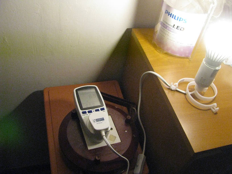
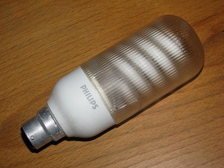
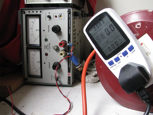
Dated : 2011-02-15 This was the very first set of LED bulb that I have tested. My boss actually wanted to showcase LED bulb in our smart home.
The power consumption is a bit lower, but the Philips LED bulb price is quite high. The price that I have purchase at that time is about $40++. This is about 8-10 times price difference when compared to a CFL bulb (compact fluorescent lamp, or energy saving bulb). These LED bulb do generate some heat. You can easily see it from the way the bulb is designed. Between the bulb and the screw, you can find the heavy chunk of metal. This is actually the heatsink which helps to dissipate the heat from the bulb. The lamp uses high power LED. These LED can generate very bright lights, but at the cost of the heat produce. Not all the electrical energy is converted to lights.
|
|||||||||||||
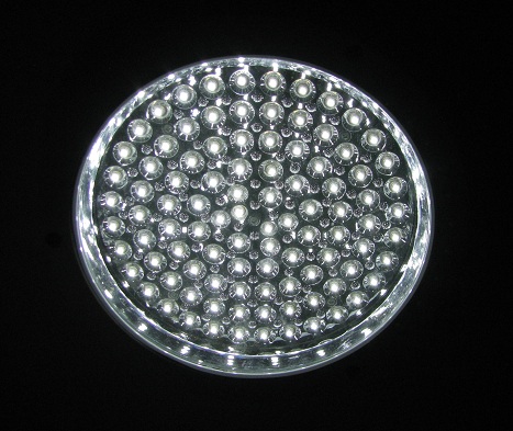
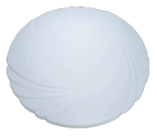
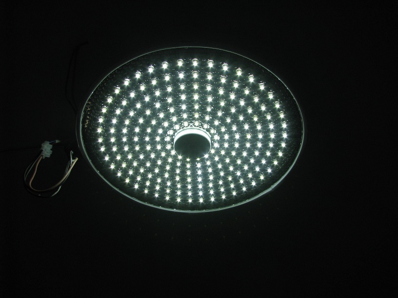
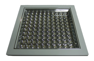
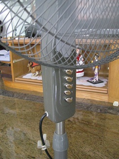
LED Ceiling Lamp Product code: LEDCL2417
LED Ceiling Light (Surface, Round, 98*LED)
available from
saveOne Pte Ltd, Singapore, www.saveone.com.sg
|
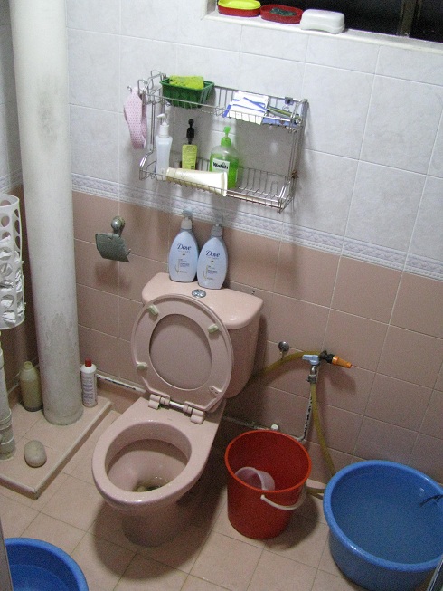
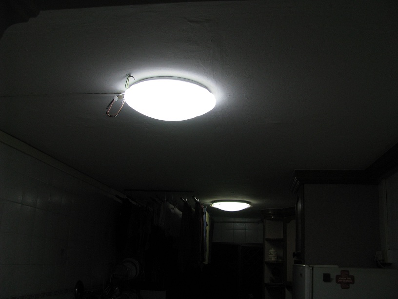
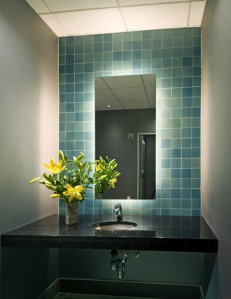
My home toilet is bright using the LED ceiling lamps. (Installed on Jan 2012)
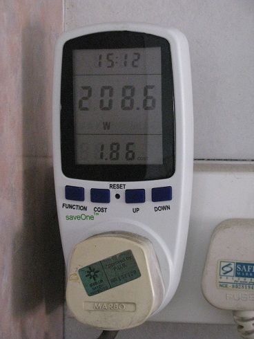
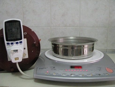
The LED ceiling lamps is make up many small LED bulbs. This 8W LED ceiling lamp provide brighter illumination at the center than the old CFL. The old 18W CFL (E27 base) that I used to have provides a brighter illumination on the ceiling than the LED lamp. There are pro & cons. LED is rather directional which is why the ceiling looks darker. However lightings to the floor area is very bright. This LED ceiling lamps uses many little low power LED bulbs. The heat generated by these low power LED bulb is insignificant when compare to the fluorescent lamp. They do not generate heat, and no heat sink is required. The low heat lighting also means that the components and material can last longer when compare to heat generating lighting technology. In short, low power LED lightings is more efficiency compare to high power LED, fluorescent and other lighting technologies. Measurement (for 8W LED ceiling lamp)
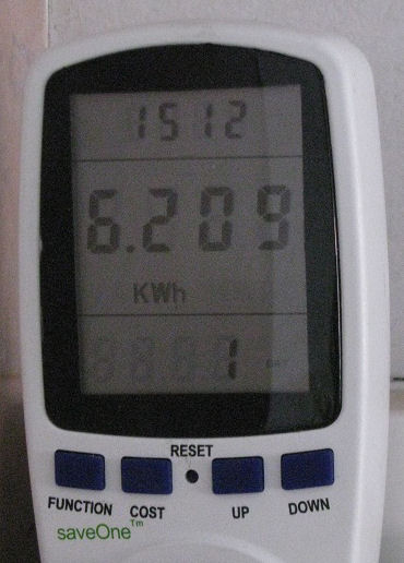
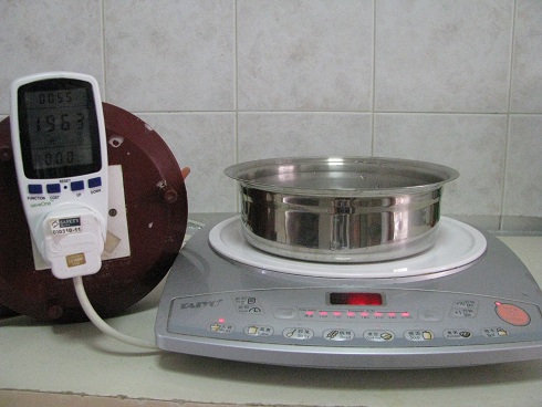
Measurement (my old 18W CFL bulb that was used to be in my toilet) Wattage: 18.3W There are other type of LED lamps that uses high power LED. These lamps uses only a few high power LED bulbs but can dissipate quite high heat. High power LED requires a heat sink (usually aluminium material) to be attached which helps to disspate heat.
|
|||||||||||||
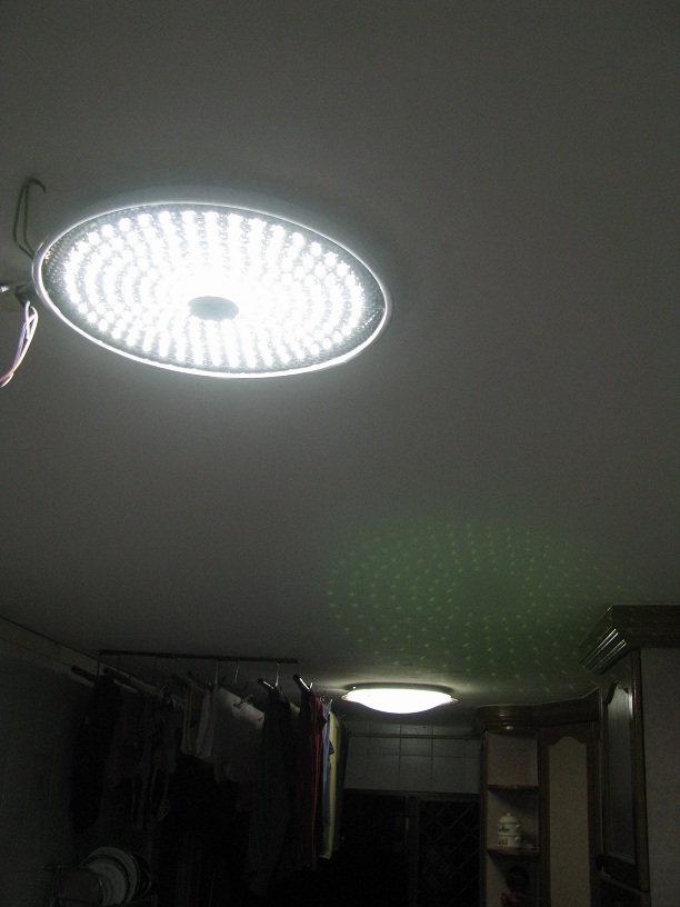
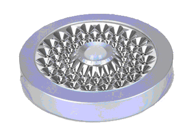
LED Ceiling Lamp Product code: LEDCL4015
LED Ceiling Light (Burger, Round, 208*LED)
available from
saveOne Pte Ltd, Singapore, www.saveone.com.sg
|
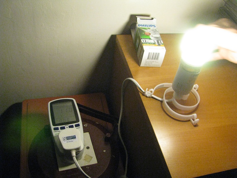
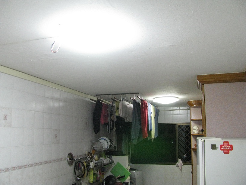
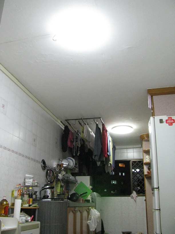
2012-05-16 Upgrade My Kitchen Ceiling lamp. I have been using the saveOne electronics ballast to power up my 2x kitchen’s ceiling fluorescent lamp for about 2 years. I wanted to change these fluorescent tube to LED but they are still functioning good. Finally one of the fluorescent (I think it is at least 5 years old) dies off. The very next moment, I ordered 2x LED ceiling lamps. Finally my kitchen is upgraded to LED. The LED lamp itself is make of plastic, and the weight is very light. It is easy to install. I have managed to reuse the mounting holes from my old lamp by drilling holes on the plastic LED lamp base.
Both my kitchen lamp used to be powered by magnetic ballast. The consume was about 40W for each lamp. The changed to electronic ballast has reduced the energy consumption to about 25-27W. The installation of LED lamp has reduce the consumption to only 15W. This is only 38% of my old 40W lamp. These LED does not generate much heat, through expected to last longer as well. Bright and efficient, I love it. Next LED lighting to go will be my rooms.
|
|||||||||||||
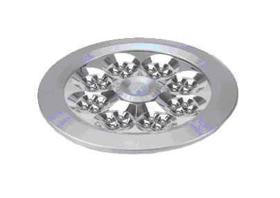
available from
saveOne Pte Ltd, Singapore, www.saveone.com.sg |
Other interesting LED ceiling lamps products. These lamps are integrated with motion & LUX sensor. The lamps gets to operates in the dark. When the lamp sense motion, it will switch on it’s LED light automatically. When there is no activity for about a minute, it will switch off the light automatically. These features makes it suitable for your storage room, toilet and corridor. |


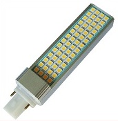
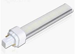
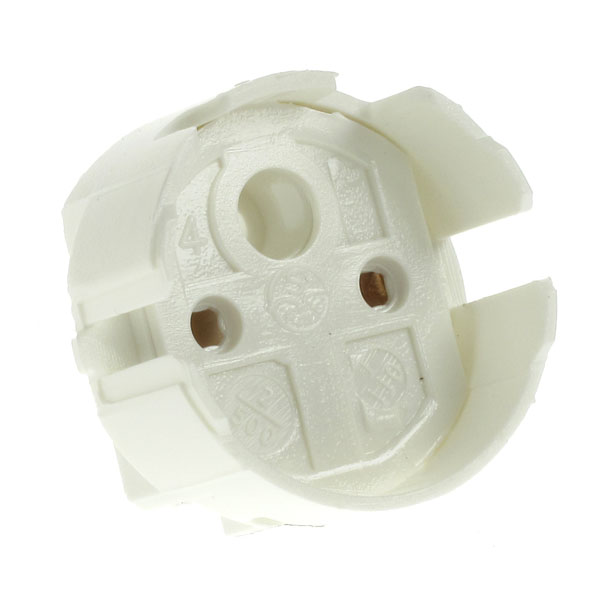
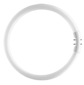
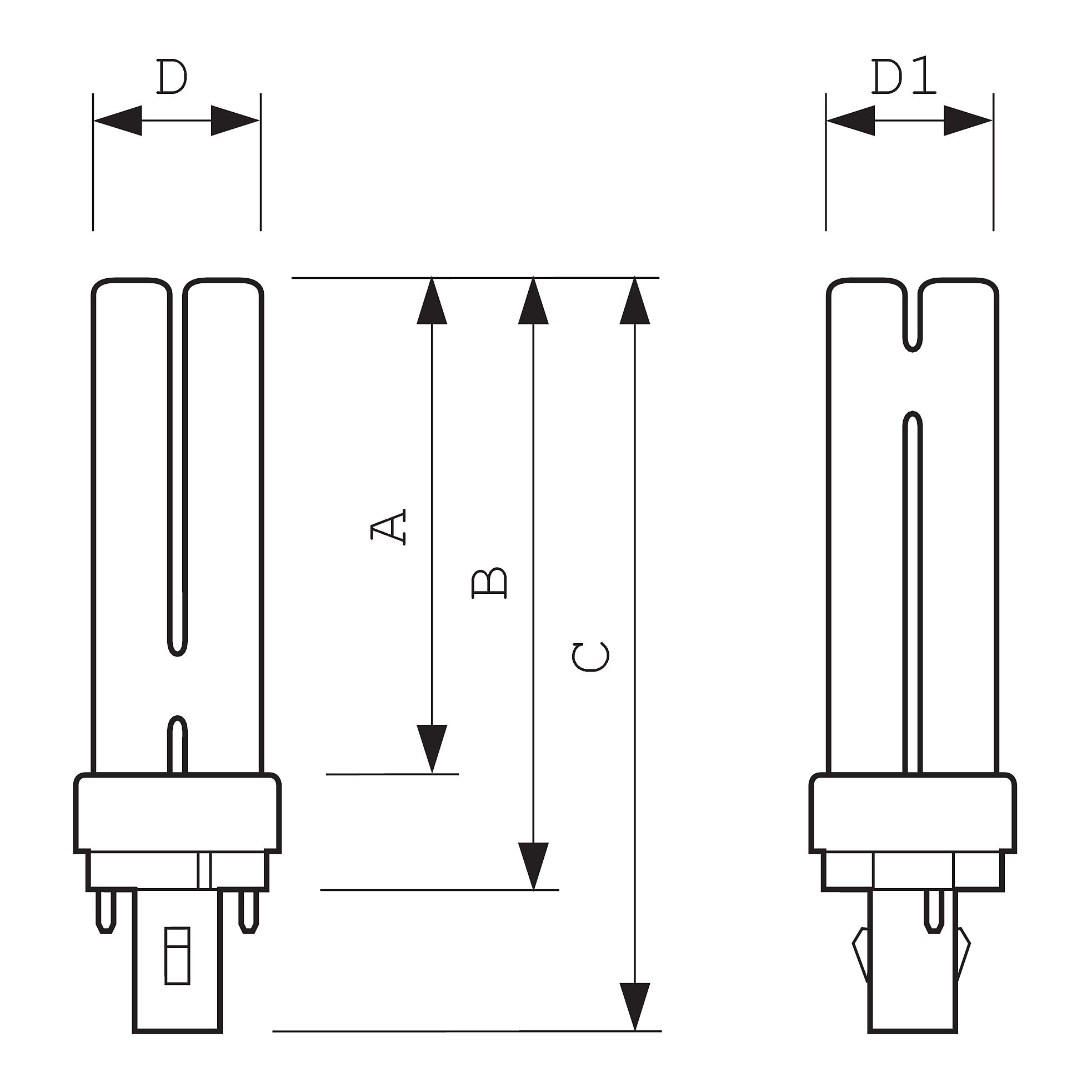
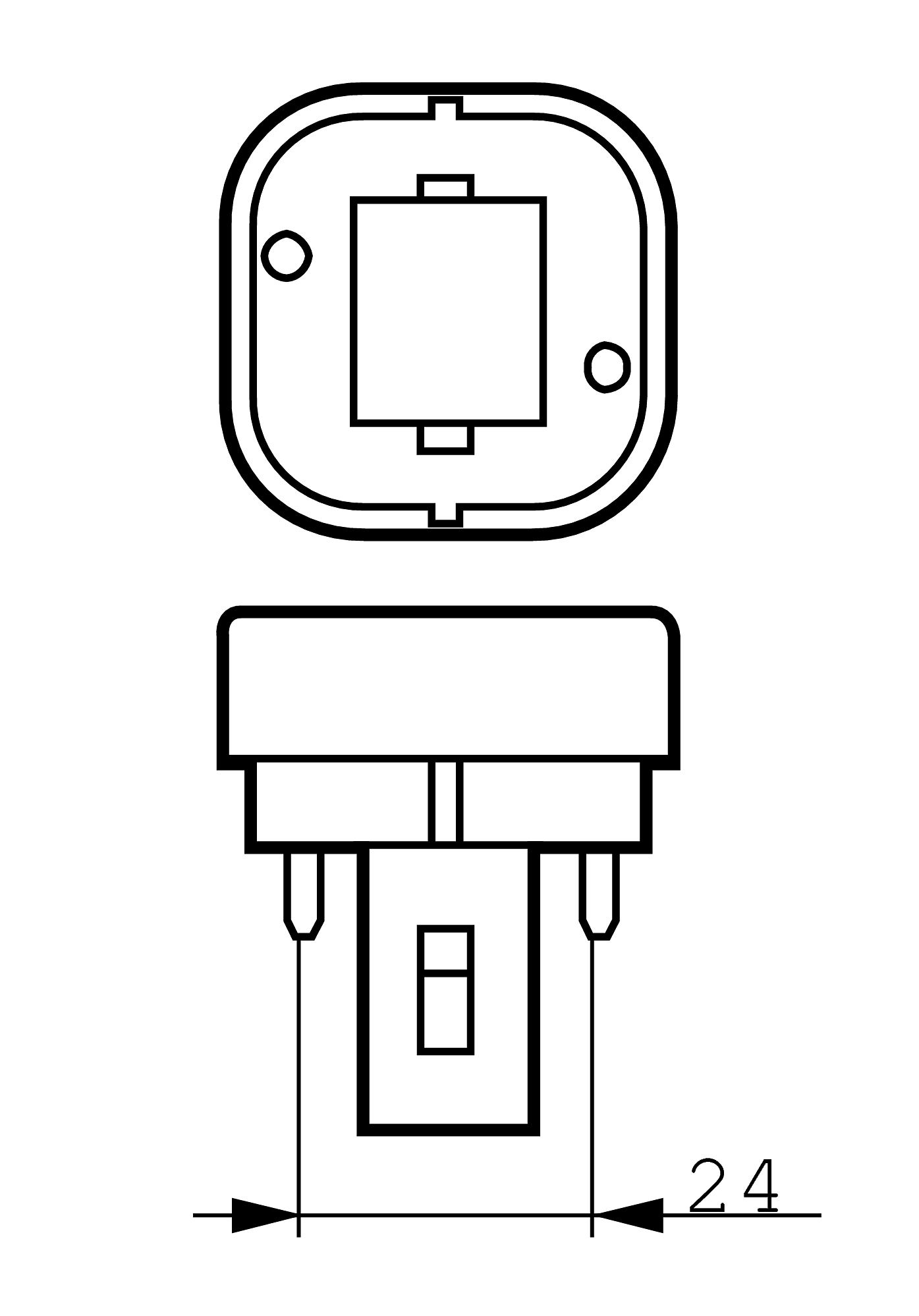
Electronic PL lamp bulb G24 base (PLC) Product code: CFLSI2154
Lamp base: G24
click here for product brochure
available from
saveOne Pte Ltd, Singapore, www.saveone.com.sg
|
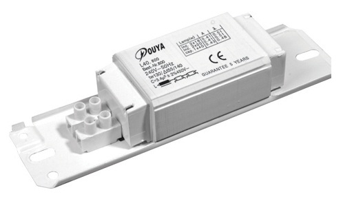
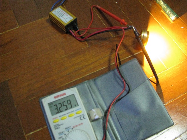
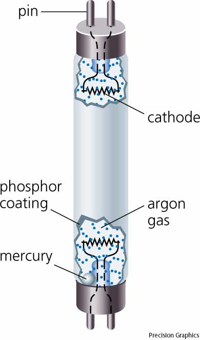
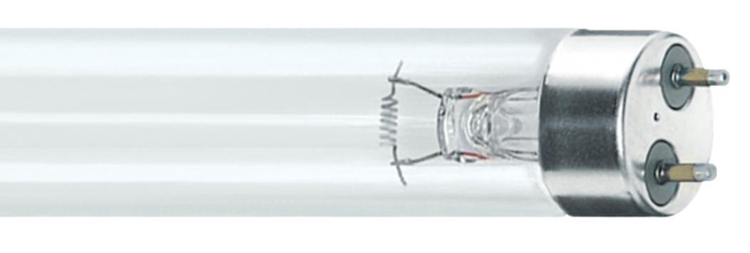
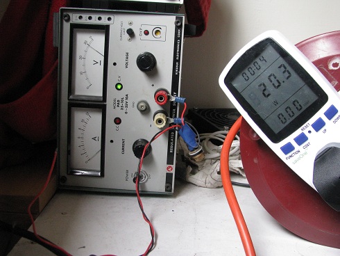
Dated: 2012-01-15 It was quite difficult for me to accept the fact that in this technological era we are still using lighting technology that are so out dated. I was not so aware about our current lighting products and technology, until I had this chance to conduct experiment on saveOne’s product. At first look, this product is no difference from the PL bulb that we normally use in our home or office building. I did not understand what is so special about this product, until I do my some market research. The current PL bulb http://www.siongboon.com/projects/2010-08-22%20electronic%20ballast/index.html The old fluorescent technology requires 3 components to work. a starter This old technology has a number of disadvantage. – Use more electricity energy. The typical PL fluorescent bulb from Philips that you can find in the market does not requires external starter. Most consumer will find it a very convient product over the conventional fluorescent that requires a starter to operate. What most the consumers do not realise is that it is no difference from the old traditional inefficient fluorescent bulb. So where is the starter? The reason that you don’t get to see any starter in the setup is because the starter has already been built into the bulb itself. A typical fluorescent tube has 4 pins. PL bulb has only 2 pin because the 2 other pin is used for a mini starter installed below the tube (near the socket). This also means that if either the tube or the starter component get damaged due to wear and tear, you will have to replace the whole PL bulb. The old setup allows you to change either the starter or tube if one of them is not working. PL bulb is easy to use but there is wastage. Not that eco-friendly. A working tube can ends up in your trush bin, just because the starter that was integrated into the PL bulb was not working.
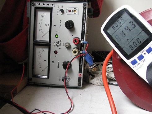
You can easy tell if you have the old PL bulb install in your home/office. The lamp will flicker on and off for a few seconds before it can be fully turned on. The flickering is actually cause by the starter’s attempts to start up the lamp. So what is so special about saveOne PL lamp? Let’s do some technical measurement, to explain the differences. This was a measurement that I took, comparing saveOne PL with a typical PL lamp + magnetic ballast.
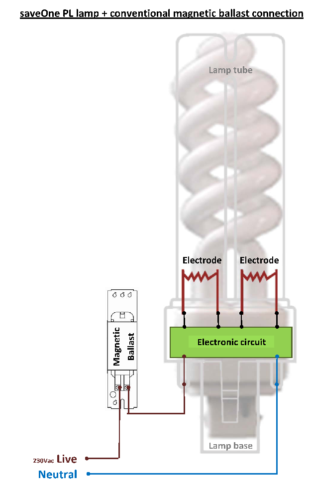
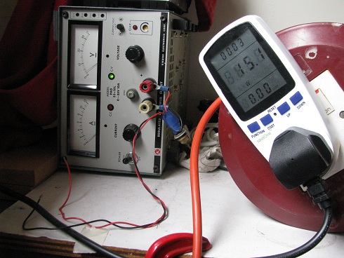
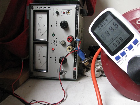
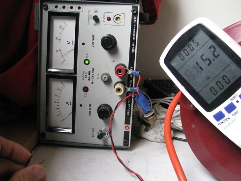
saveOne has designed the electronics to replace away with the magnetic ballast and starter system. The electronic control is more efficient consuming only 9.1W during the measurement. The PL lamp consume 9.5W at start up and drop down to 9.1W (steady state) after the tube gets to warm up. In contrast the typical PL bulb begins at 13.9W and rise up to 14.3W during the steady state. saveOne PL lamp is driven by electronics. Users do not need to worry about the type of ballast to match with the lamp. The magnetic ballast PL bulb has a typical higher wattage consumption; this is especially true if the magnetic ballast is not match to the fluorescent tube wattage. In some cases, it wattage consume can even be higher. For the best efficiency in brightness, power consumption and lamp’s lifespan, the typical PL lamp has to match with the ballast of the correct wattage. The current drawn by the magnetic ballast setup is also higher at 0.158A. Compare to the saveOne PL bulb 0.066A, it is about 2.4 times higher. The reason why a magnetic ballast draws more current is because of its inductive nature. Inductive load is actually an energy storage device and will draws/returns more current than its actual consumption. Unconsumed energy will be returned to the grid. This results in a higher current flowing through the magnetic ballast. The higher current flowing through a finite cable diameter will generate heat compare to a efficienct bulb that uses less current. These are actually energy losses. If you attempt to touch a magnetic ballast after switching your lights on for about 10 minutes, you will feel how hot it can be. The power factor for the saveOne PL bulb is high at 0.63; the reason for the low current drawn. Power factor of 1.0 (which is the maximum possible reading) indicates that a device will draw the actual current it needs for its operation. Higher power factor means better efficiency. The heat generated from the magnetic ballast is a waste of energy, and will tends to wear out the various component more. The heat will have indirect impact on the environment temperature and aircon electrcity wastage as well. If you feel the heat surrounding the old PL bulb, you can feel the heat. When you change old PL bulb, you might also find that the tube has the tendency to drop off from the base or the glass tube can break easily. These wear and tear can also expose the dangerous mecury content inside the florescent tube, which will contaminate your home/office environment. saveOne PL lamp uses electronics to switch the fluorescent lamp. The higher operating frequency also plays a part in the efficiency of the lamp. The saveOne PL bulb replacement over the old PL bulb is easy. There is no need to do any rewiring. Simply change the bulb. The electronics built into saveOne PL lamp is able to work with existing installed magnetic ballast. I was sceptic about its claim and also did a measurement on its performance when it is used with a magnetic ballast. Measurement (for saveOne 10W PL bulb + magnetic ballast) The result was quite unexpected when I first do the measurement. The performance is even better without removing your existing magnetic ballast. This product is designed specially for consumer using the old magnetic ballast PL lamp, helping them to switch over to a more energy efficient saveOne PL lamp.
Even though the magnetic ballast was installed with the saveOne bulb, it does not generate much heat as compared to the old PL bulb. This is much expected with the low current that the bulb is drawing. saveOne tube is designed in a spiral shape which allow more lights to be projected out. The fluorescent tube also contains triphosphor material which allows the tube to generate brighter light using less electricity energy. This patented product from saveOne really earns my respect for the innovation that they have put in the area of energy saving. It changes my views about the old lighting technology that we are still using in Singapore. Many places are still using the olf PL bulb.
See the following comparison table for more information.
Buy this Energy Saving PL Lamp Now at the PIC-store
|
|||||||||||||||||||||||||||||||||||||||||||||||||||||||||||||||||||||
Comparison among various energy saving lightings for PL fluorescent lamp. (updated Jan 2012)
footnote: |
||||||||||||||||||||||||||||||||||||||||||||||||||||||||||||||||||||||

 and a fluorescent tube
 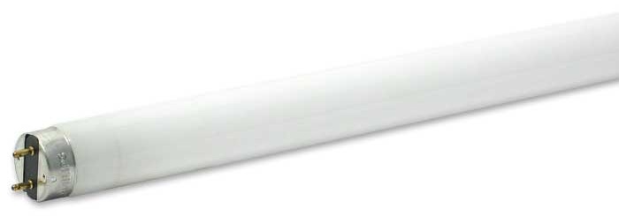 to work.
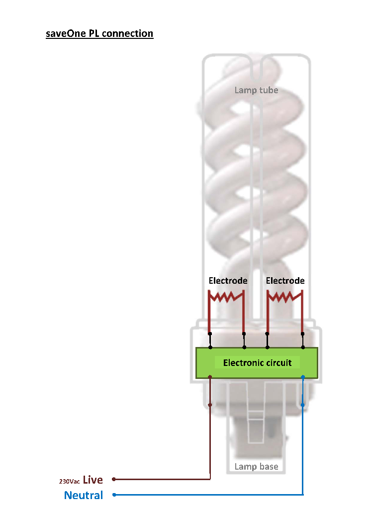

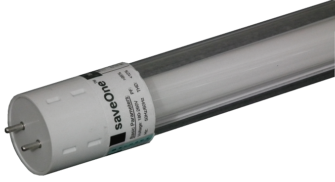
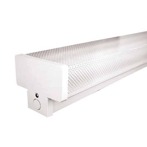
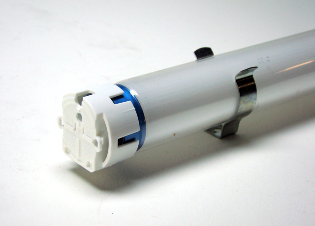
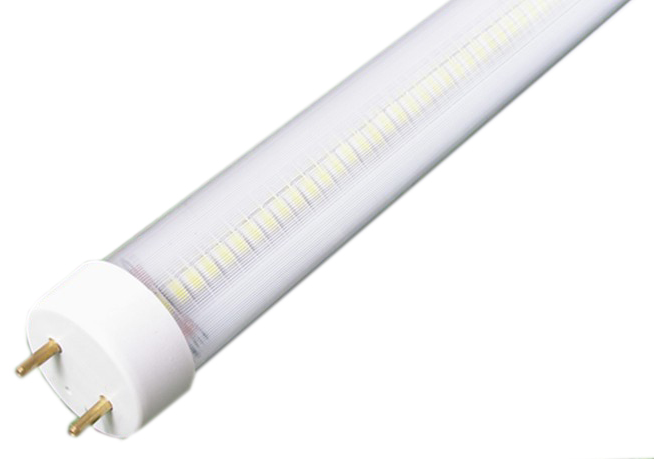
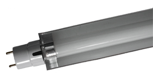
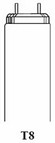
Energy Saving T8 fluorescent tube SuperTube Product code: FLRSL1644 Lamp base : T8 click here for product brochure
available from
saveOne Pte Ltd, Singapore, www.saveone.com.sg
|
When
I first got to know of this energy saving T8 fluorescent tube, it looks
just like any ordinary T8 lightings. I have learned over a series of
measurements and experiements that this is no ordinary T8 fluorescent
tube. It has the performance comparable to a LED T8 tube, but at a cost
much lower. The design also overcome some of the shortcoming of an
ordinary fluorescent tube that are available in the current market.
These have make it one of the most efficient and economical lighting
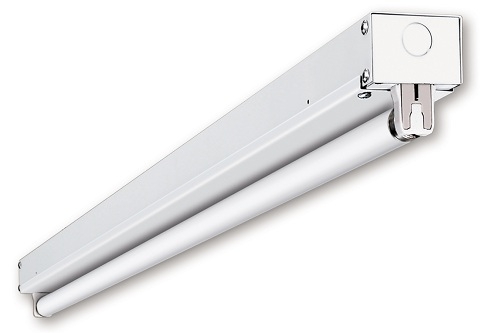
tube among the rest (LED T8 and T5). Normal T8 housing can be very bulky. Magnetic ballast, starter and starter holder are housed inside the enclosure.
Space saving T8 fluorescent tube socket for direct electrical connection. Useful for ceiling/wall cove lightings where space are very tight. Setup is cheaper as well without the enclosure, starter, starter holder and magnetic ballast.
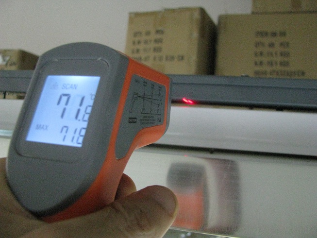
The product’s built-in integrated ballast is also designed to work with your existing magnetic ballast. This means that you do not have to change any wiring or remove the magnetic ballast from your existing setup. Simply change the old T8 tube with this new energy saving tube, and remember to remove away the starter. The new lamp turns on its light instantly without the need for any starter. You might wonder that with the magnetic ballast working together with this new product, will it affect the energy consumption? I had the same thought as well. Measurement were taken. By using the magnetic ballast together with the product, it has insignificant changes to its performance and energy consumption. In fact the power and current drop a bit. These can be explain by the measurement result which will be presented shortly. The power factor of the ordinary T8 tube setup is poor. This is mainly due to the magnetic ballast which is an inductive component (which is only wire coil). The poor power factor results in higher current being drawn from the electrical grid. The current drawn is 4 times higher than the saveOne’s T8 energy saving product. With such a high current flowing through the magnetic ballast, it will generate heat. This is also why it feel burning hot when you try to touch the magnetic ballast which has been operating for more than 10 minutes. This is wasted energy as a form of heat. The heat also affect your environment temperature indirectly. In contrast, this energy saving T8 lighting product uses much less current. Less heat will be generated. Even if this low current flows through your existing magnetic ballast, it will not generate much heat. The low current is transparent to your existing magnetic ballast; there are no loss.
The following measurement result shows that the power consumption for the saveOne T8 product is almost the same as a typical LED T8. Given the similar performance, the ROI (return of investment) of the product will be much better because the LED cost is high.
Note: wattage various around 36W- 45W depending on the magnetic ballast
The product has indeed impressed me for its efficiency when compared to a LED T8 tube. I have also done up a product comparison table to compare against other type of lightings solution to replace the old T8 magnetic ballast fluorescent lamp. See the followings for more information on the comparison between more types of alternative replacement solution for T8 lightings. |
|||||||||||||||||||||||||||||||||||||||||||||||||||||||||||||||||||||||||||||||||||||||||||||||||||||||
Comparison among various energy saving lightings for T8 4FT fluorescent lamp replacement. (updated Jan 2012)
footnote:
|
||||||||||||||||||||||||||||||||||||||||||||||||||||||||||||||||||||||||||||||||||||||||||||||||||||||||
Comment: As based on the comparison among various lamps technology, the latest energy saving LED and SuperTube lamp are both very energy efficient lamp. LED is known to last longer than the fluorescent technology but the cost of the lamp is much higher. That is why the ROI (return on investment) is poor when compare to the fluorescent technologies. The fluorescent technologies have similar ROI although the cost price is different. This is because the new fluorescent design has achieved an efficiency close to the LED technology.. SuperTube design has a cost slightly higher, but it offer more electricity saving, with a better protection against mercury contamination than the other fluorescent technology. In terms of cost and efficiency, the SuperTube lamp offers a better choice over the lamps. If you are interested to find out about saveOne’s SuperTube lamps, you can contact them or visit their office for a demonstration or an experiment experience. |
||||||||||||||||||||||||||||||||||||||||||||||||||||||||||||||||||||||||||||||||||||||||||||||||||||||||


Product picture taken from ![]() and
and ![]()
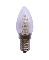
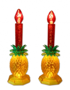
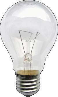
LED candle and chandelier bulb (compare to incandescent bulb)
Lamp base: E12, E14
available from
saveOne Pte Ltd, Singapore, www.saveone.com.sg |
I love these LED candle bulb. These E12 bulbs are usually used for the praying lamp on our Taoist altar table. It simulate the olden days of using candle flame..
Compare to the normal incandescent bulb 16W, these LED bulb only uses 0.3W. That is about 50 times saving in energy. The incandescent bulb can be very hot after turning on for a few seconds, and these can be quite dangerous especially with naughty children running around the house. These LED bulb remains cool after operating for the whole day. The lifespan of these LED bulb is much much longer compare to the incandecent version.
The old incandescent bulb cost less than a dollar, a lot cheaper then the LED bulb which cost about S$5 to S$8. Considering the 16W energy that the incandecent bulb will consume, it will actually cost more to maintain it. This is even more significant if you operate the lamp for 24 hours per day. The electricity bill that you save within 2 months of operation can easily help you recover the cost of the LED bulb purchased. Per bulb would have save you about S$3 to 4 base on the electricity tariff rate of S$0.30/Kwh. Lifespan of incandescent bulb can be short, as the heat and frequent switching on/off can burn off the filaments inside. For these LED bulbs the brightness is lower and will not be suitable if you have a lamp covering. The cover will reduce the brightness. Considering the energy saving, temperature, safety and lifespan that this LED bulb brings, it is a much more economical choice over a incandescent bulb.
Buy this LED Candle Bulb Now at the PIC-store
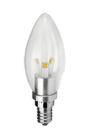
Another great bulb that I will like to introduce is the LED chandelier bulb which uses only 3W compare to the incandescent version which uses 40W.
This LED incandescent chandelier bulb uses a high power LED. The light is very bright and look very much like the incandescent bulb’s filament. The high power LED bulb do generate some heat but it is a lot less than the incandescent version. This LED bulb 3W uses about 13 times less energy than the conventioanl incandescent bulb of 40W. These LED bulbs are worth recommending for their higher effciency, lower heat generated, safer and longer life span over the conventional incandescent bulbs.
Buy this LED Chandelier Bulb Now at the PIC-store |


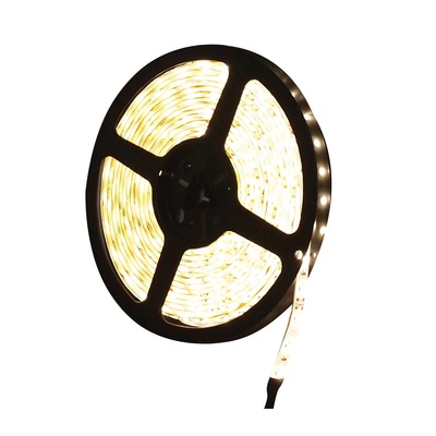
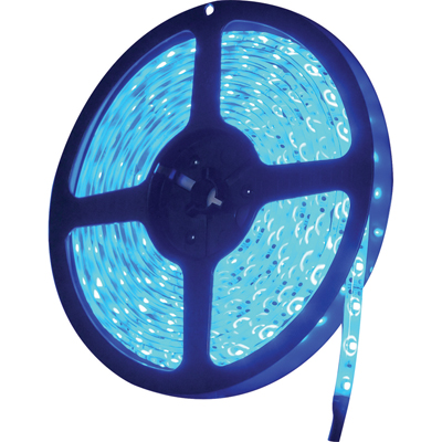
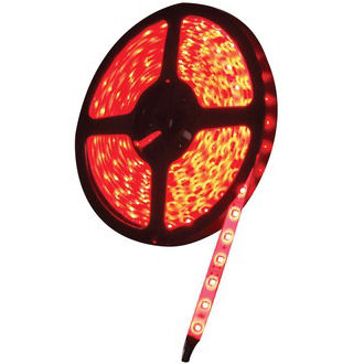
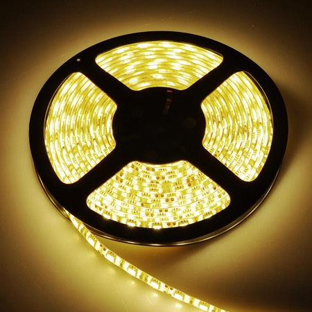
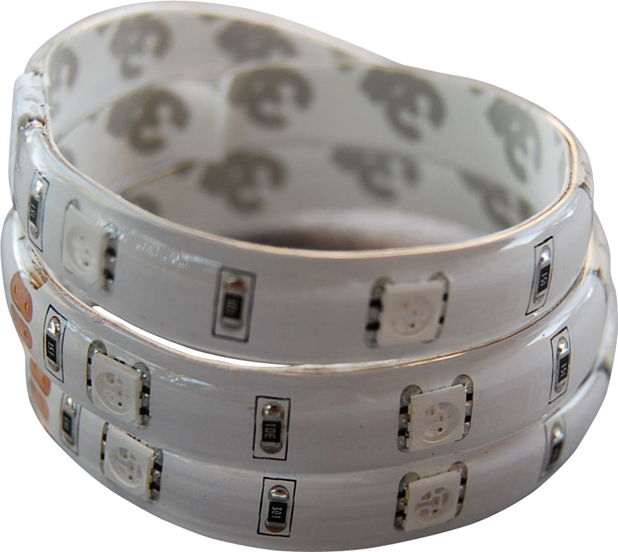
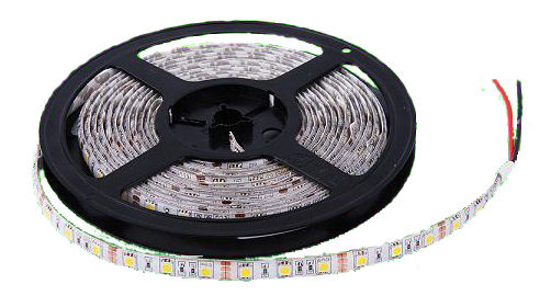
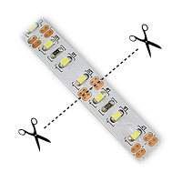
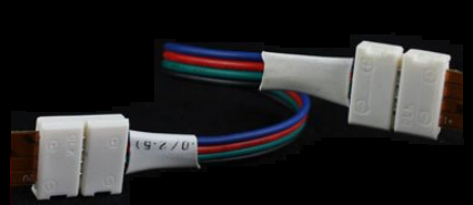
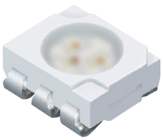
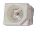
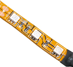
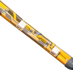
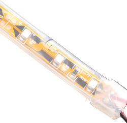
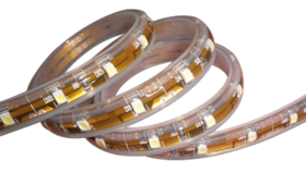
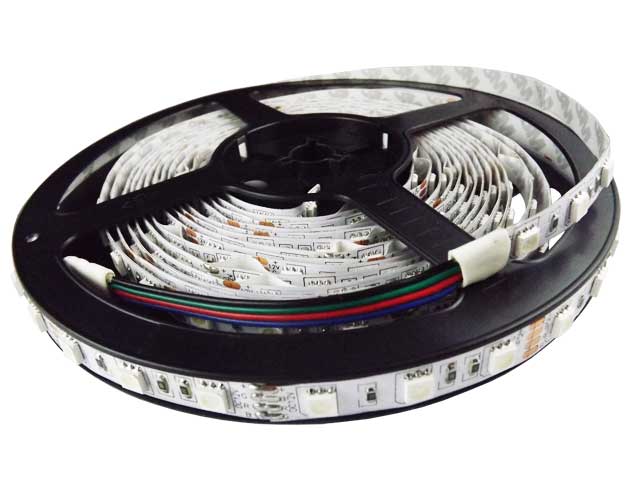
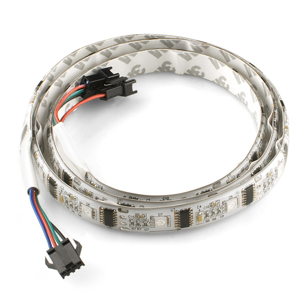
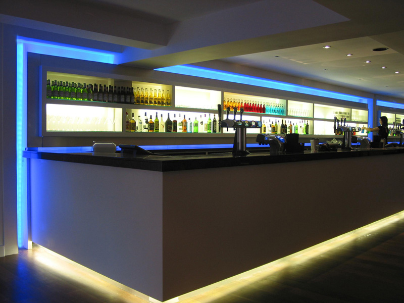
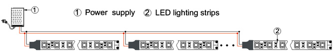
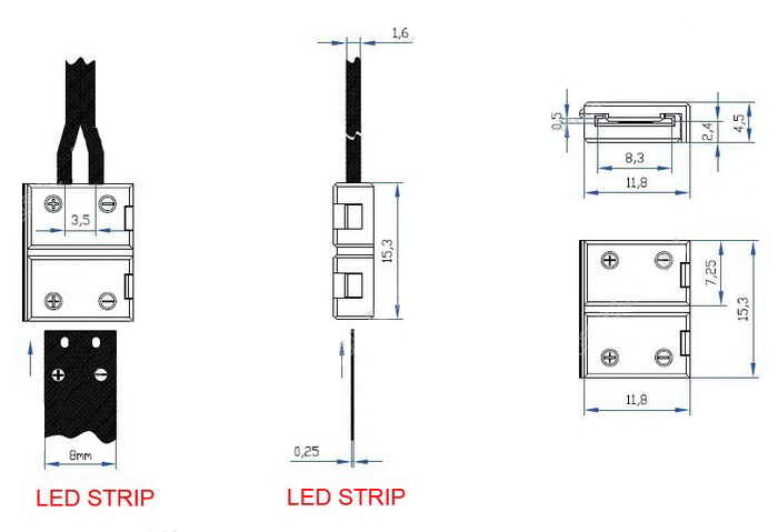
LED lighting strips
Lamp base: Bare wire strip 1meter/reel, 50mm cuttable section 30/60/120 LED per meter
|
Last updated: 2012-03-13 LED strip is getting more and more popular nowsaday. Unlike other lighting, the led strip is very flexible allowing it to bend over corner and curve. They usually comes in a roll of 5m per reel and can be easily extended or cut to length in a section of 50mm.
The installation and wiring is very simple. It using a low voltage of 12V which is very safe to handle. There are also strip using 24V. You will not get electrical shock by touching the pair of 12V wire using your bare hand; neither will it cause nasty short circuit when it gets in contact with water. This make it suitable for installation near water or where it can easily get in contact with water or the user. Special area like toilet basin, aquarium tank lighting, floor area, bed side and lower section of the cabinet. It is much safer than any 230Vac lighting; about 20 to 30 times lower. There are many style of installing the strip. You can lay the strips simply on the shelf. Some strips has sticker/adhesive tape on its back, allowing it to sticks itself to most surface. Remember to clean the surface before sticking the strips on it. There are also accessories which you can extend or secure the strips. The strips allows installation where traditional lamp installation is not possible.
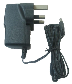
The strip is usually drive by a 12V switching regulator or power supply adpater. Like a battery, you should never short the positive and negative terminal of power adapter; the adaptor can be damage. A 12V power supply adaptor comes in various current rating. A longer strips requires more energy to light up, therefore a higher current rated power supply will be needed to drive it. A meter of 14.4W strips requires about 1.2A. If you are getting 3 meter, the current needed will be about 3.6A. The power adaptor that will be required has to be a minimum of 12V 4A. Usually I will give the power adapter more buffer. A rating of 12V 5A or more will be safer. If you use a lower current rated supply, for example 12V 2A, you will likely to cause internal damage to the power adaptor. Higher current rated power supply is better in performance, but is generally more expensive.
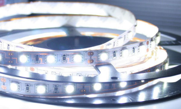
LED strip circuit is a relatively simple design. It is unlikely that you will damage the strip using a wrong rated power supply. Even if you connect the positive/negative priority in reverse, neither the strip nor the power supply will be damaged. The strip operates on 12V, and can tolerate minor voltage difference (10-13V). A voltage too high applied to the strip can damage the LED bulb. There is a limit to how long the strip can be extended. 10m is the recommended maximum continous strip length. Extending it longer, you will find that the light intensity near the far end of the strip will become much dimmer than the other end that is near the power source. If your eye are sharp enough, you should notice the intensity difference within a 5m long strip itself. This flaw is due to the slim and narrow strip design (resistance), restricting the high current flow, preventing current to reach to the far end of the strip. The high resistance on the strip design also result in slight heat generated. This problem is more obvious with the high power strips. You can improve the intensity at the far end of the strip by connecting the end back to the power supply. This will allows the current to reach the far end of the strip directly, without passing through the whole LED strips. To achieve a more consistant intensity, it is recommended to connect the strip in a shorter section of 2m each. Each 2m section should be connected directly to the power supply in a star wiring configuration. The exact current consumption of the LED strips is slightly difficult to compute because of this flaw. Depending on the strip connection in series or parrallel the consumption can varies. The exact consumption can only be determine by a current meter. In general, the computation method as introduced eariler would be more than enough to drive the strip. There are many type of strips, and they are usually classified by the following 4 characteristic. – LED bulb size (5050, 3528)– Number of LED per meter (30, 60, 120) – Strip package (IP67, IP65, IP44, IP20) – Color (Warm (2700k), Cool (6500k), other specific color) The LED bulb or chip size 5050, 3528 is actually a number code for EIA standard footprint size. These standard footprint allows PCB designer to draw the correct pad size so the the LED can be mounted properly onto the PCB board. For some reason, these code has becomes a standard when ordering LED strips. 5050 actually also defines the LED size in two dimension 5.0 x 5.0mm. For 3528, LED size is 3.5 x 2.8mm. As a general guidance, 5050 LED has bigger chip size, and is expected to have a higher intensity (brighter) and wattage (consume energy) than the 3528 chip.
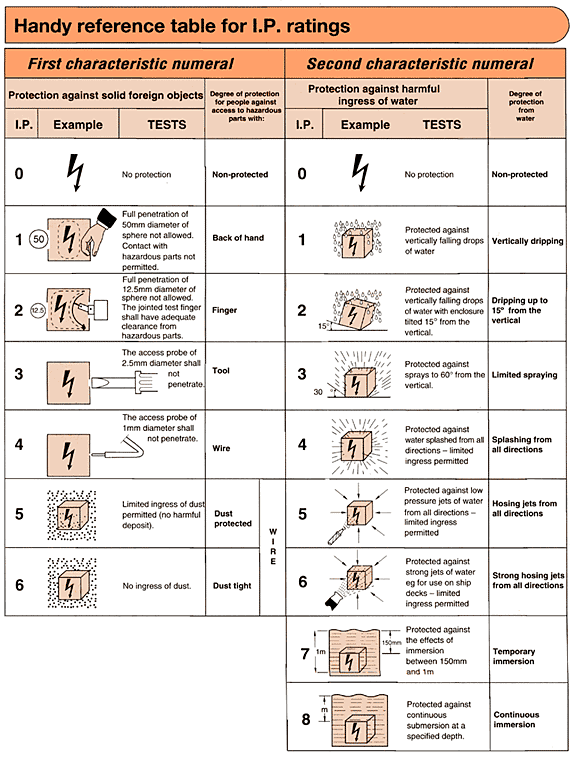
IP code (Ingress Protection Rating) is standard define a series of code to label product’s strength of resistance against dust and water.
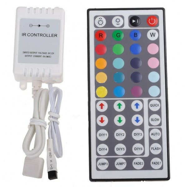
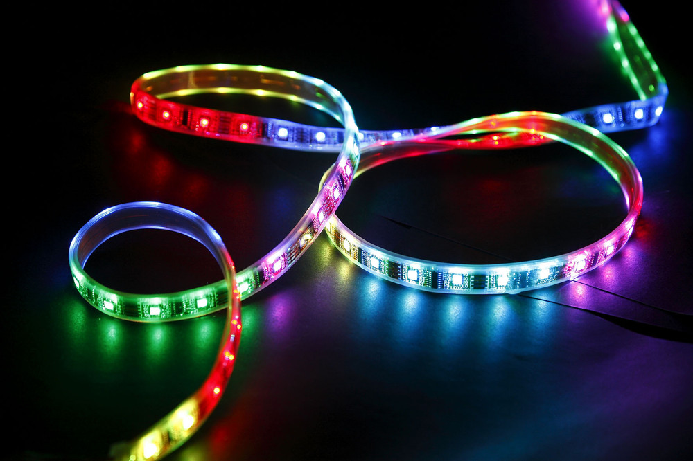
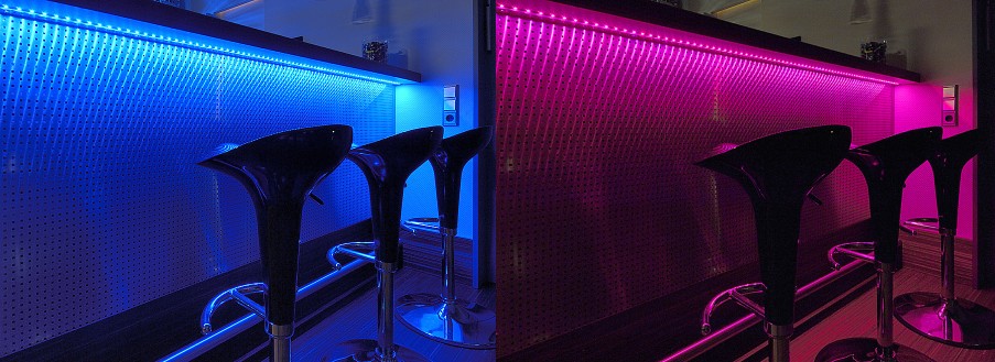
There are also LED strip that can change their color making use of RGB LED. There are also special LED strip that can generate lighting patterns. These strips will require a LED strip controller to work.
|
|||||||||||||||||||||||||||||||||||||
| Funitures |
|
|||||||||||||||||||||||||||||||||||||
| Shelf | 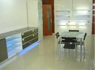 |
|||||||||||||||||||||||||||||||||||||
| Cabinets | 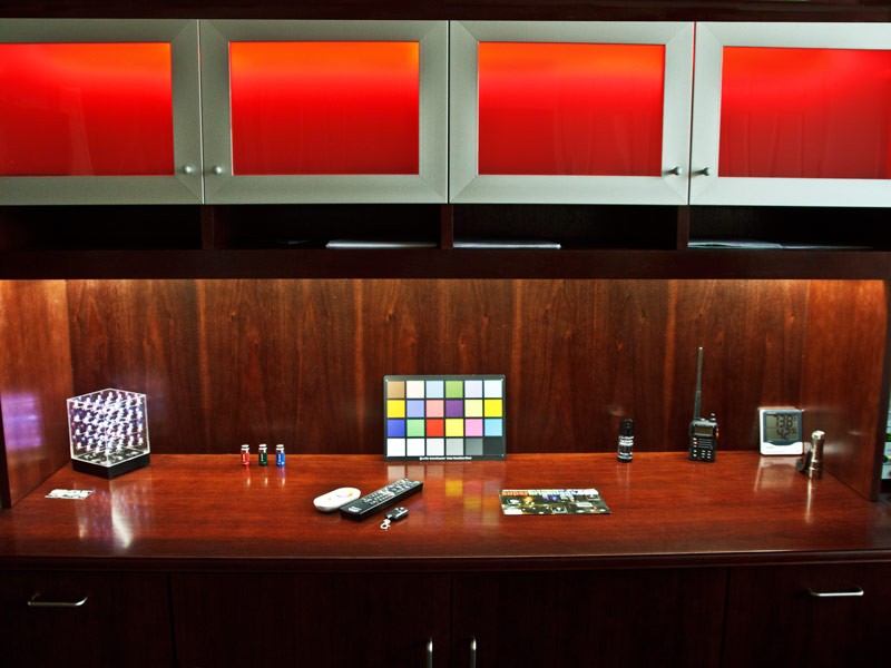 |
|||||||||||||||||||||||||||||||||||||
Below Kitchen cabinet – Provide some light during the night time |
 |
|||||||||||||||||||||||||||||||||||||
| Rised floor platform |  |
|||||||||||||||||||||||||||||||||||||
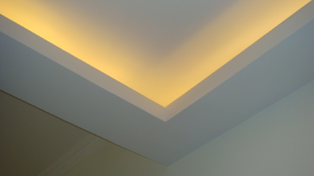
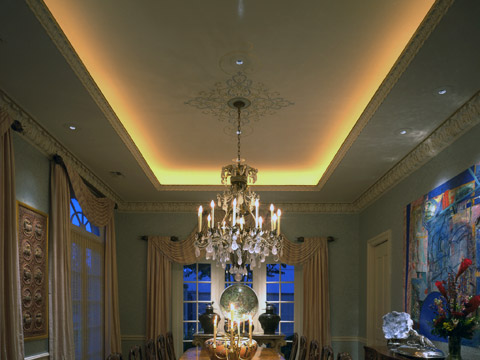
Cove lighting |
|
|||||||||||||||||||||||||||||||||||||
Toilet, and behind mirrors LED strips operate at 12V, and is safer than T5 tube which operates at 230Vac. A normal T5 tube is made of glass and contain mecury content. Installing T5 behind the mirror which is reachable can be dangerous, comparing to the LED strip. The LED strip when submerge in water will not result in electrical short circuit. This will not be true for T5 tube. |
|
|||||||||||||||||||||||||||||||||||||
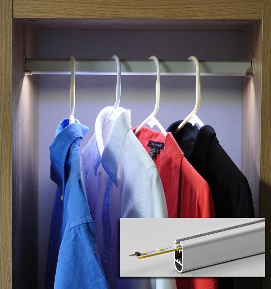
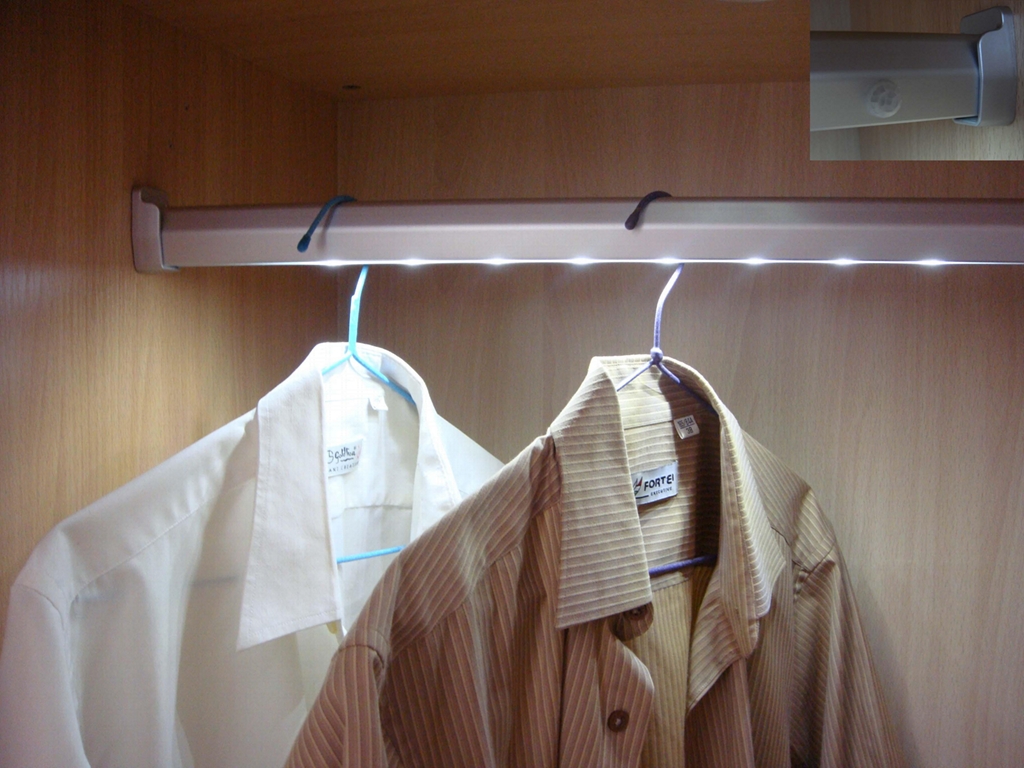
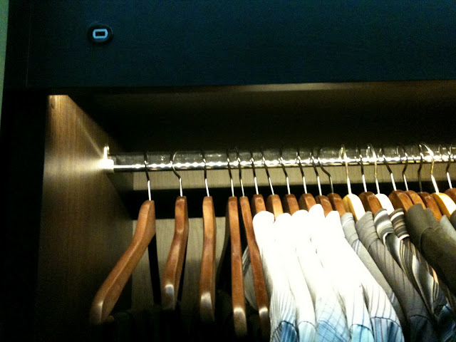
Wardrobe LED strips is slim and safe, allowing installation in tight space such as a closet or cabinet display. |
|
|||||||||||||||||||||||||||||||||||||
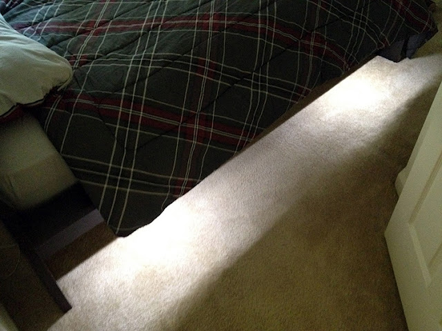
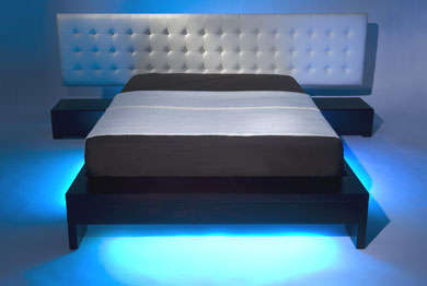
| Along or under the bed |
|
|||||||||||||||||||||||||||||||||||||
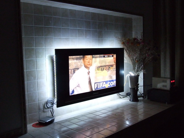
| TV console |
|
|||||||||||||||||||||||||||||||||||||
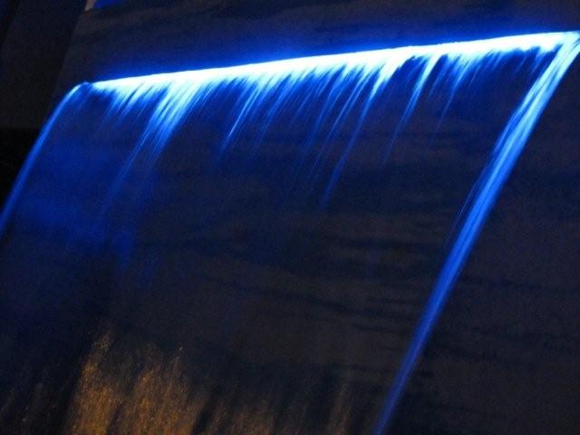
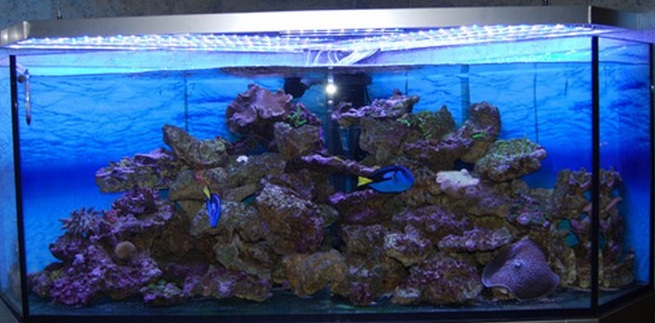
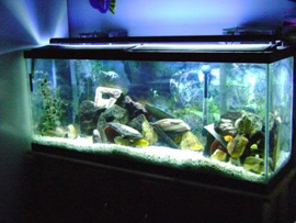
| Water features |
|
|||||||||||||||||||||||||||||||||||||
| LED strips for aquarium. If the tank is deep, more strips may be required for the light to penetrate deep into the water. |
|
|||||||||||||||||||||||||||||||||||||
| LED strip lights for plant |  |
|||||||||||||||||||||||||||||||||||||
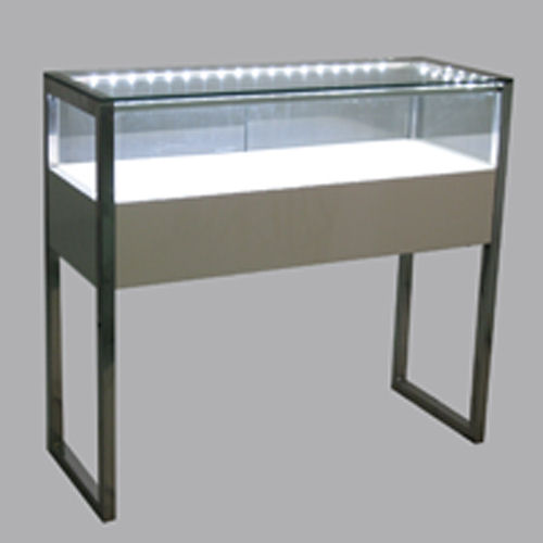
| Jewelry showcase |
|
|||||||||||||||||||||||||||||||||||||
| PIR motion sensor accessories for LED strip | 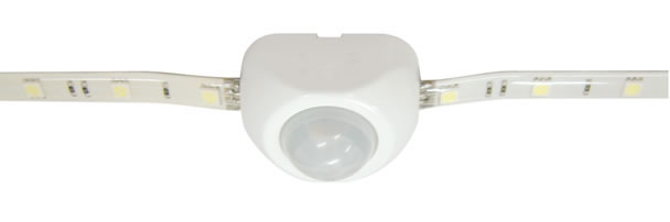 |
|||||||||||||||||||||||||||||||||||||
| LED strip installation guide |
|
|||||||||||||||||||||||||||||||||||||
reference: http://jacksledprojects.blogspot.com/2011_10_01_archive.html |
||||||||||||||||||||||||||||||||||||||


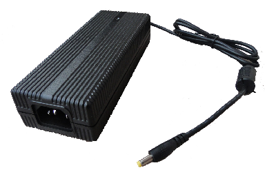


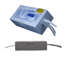
LED driver
|
Typical LED driver rating |
|||||||||||||||||||||||||||||||||||||||||||||||||||||||||||||||||||||||||||||||||||||||||
Typical LED driver specification.
|
|
|
||||||||||||||||||||||||||||||||||||||||||||||||||||||||||
This is meant to be a general reference for various lamp technology available on the market. The following information is not comprehensive for a detail one to one comparison.
footnote:
|
||||||||||||||||||||||||||||||||||||||||||||||||||||||||||


Manufacturer for Halogen and incandecent lamp products.
|
|
|
||||||||||||||||||||||||||||
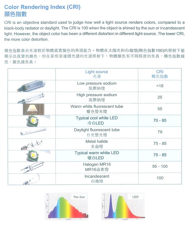 |
Defination used in Lightings
Color Temperature References: http://www.feit.com/education/feitcolortemperature.html |
||||||||||||||||||||||||||||
 |


|
reference: – http://www.answers.com/topic/fluorescent-lamp
|
|
||||||||||||||||
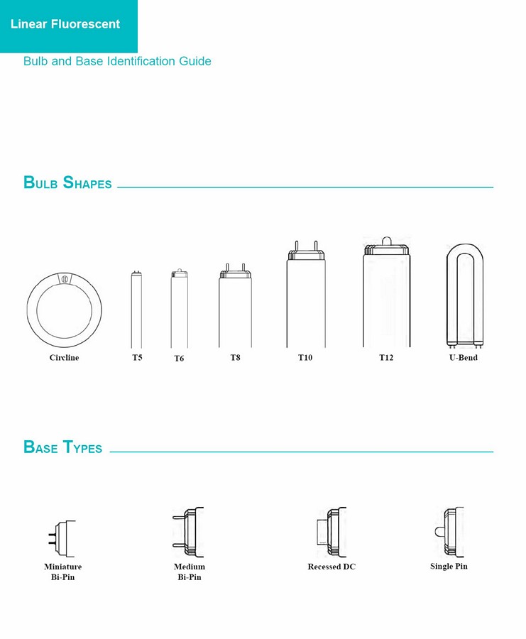
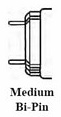
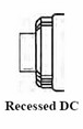
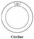
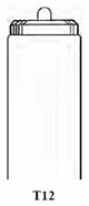
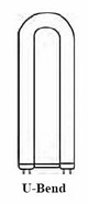
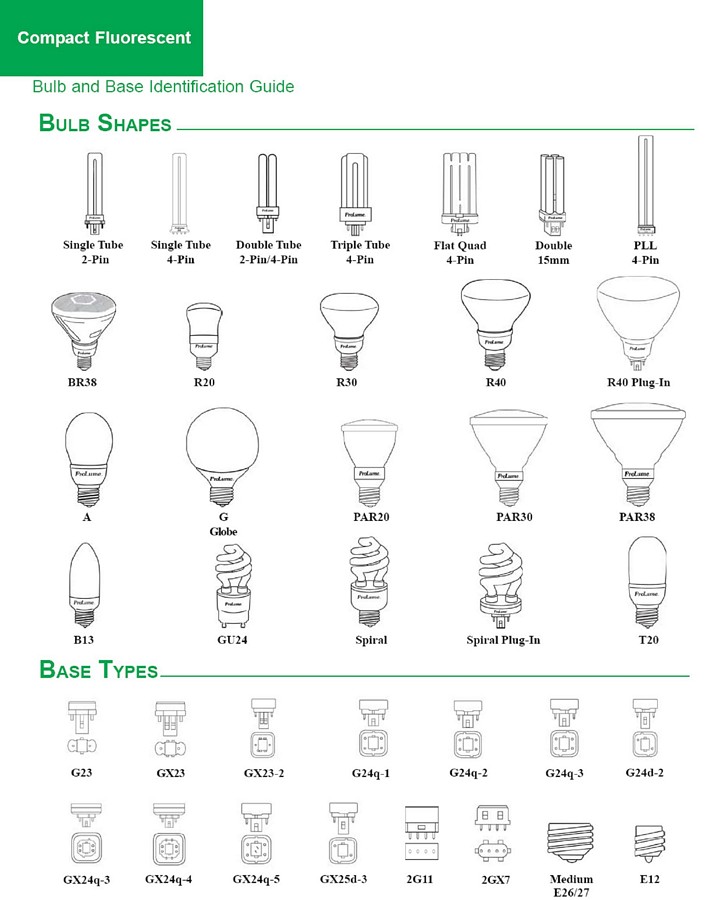
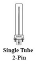
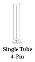
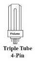
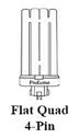
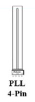
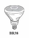
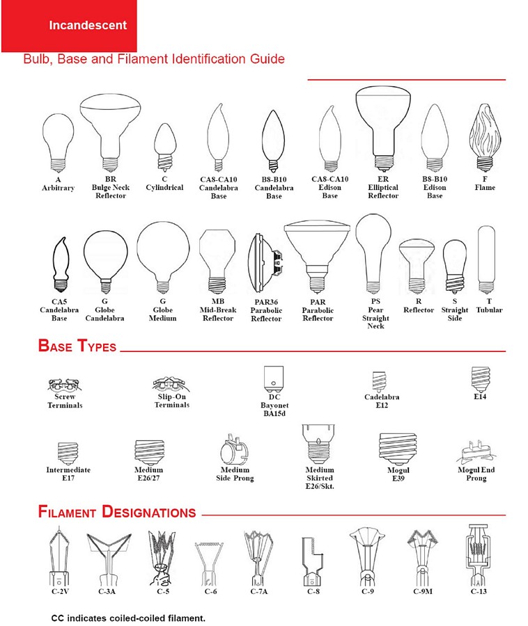
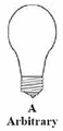
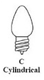
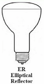
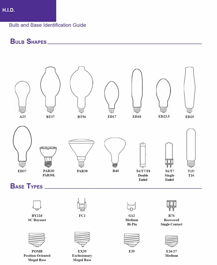
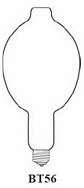
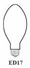
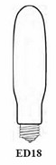
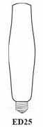
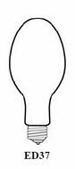
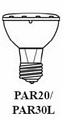
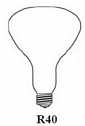
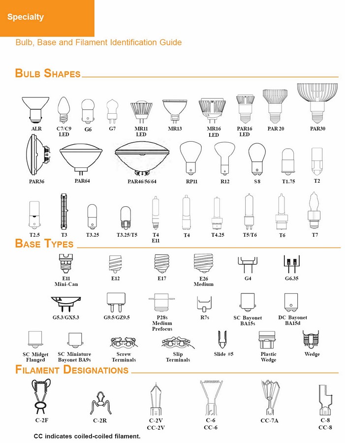
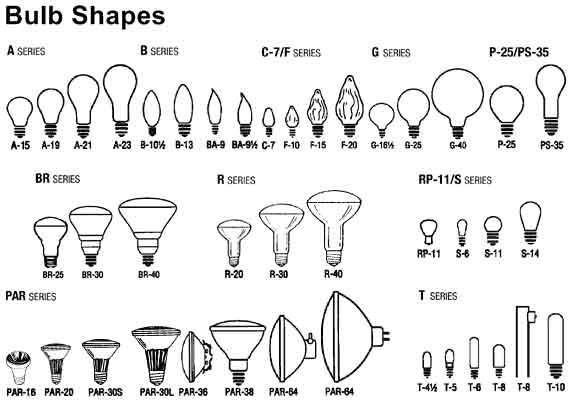
Bulb Shapes
Singapore commonly used bulb shape & base is highlighted in bold font. |
|
||||||||||||||||
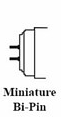
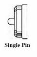
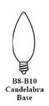
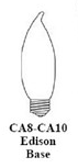
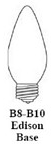
Base Types
Singapore commonly used bulb shape & base is highlighted in bold font. |
    |
||||||||||||||||


|
reference: |
 |
|
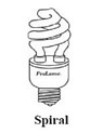
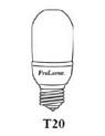
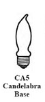
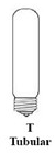
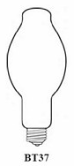
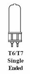
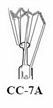
Bulb Shapes
Singapore commonly used bulb shape & base is highlighted in bold font. |
|
|
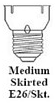
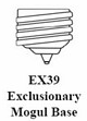
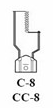
Base Types
Singapore commonly used bulb shape & base is highlighted in bold font. |
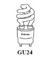
G24 lamp & socket |


 |
||
Bulb Shapes
Singapore commonly used bulb shape & base is highlighted in bold font. |
|
|
Base Types
Singapore commonly used bulb shape & base is highlighted in bold font. |
|
|
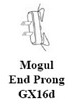
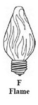
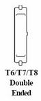
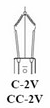
Filament Types
Singapore commonly used bulb shape & base is highlighted in bold font. |
    |


 |
||
Bulb Shapes
Singapore commonly used bulb shape & base is highlighted in bold font. |
|
|
Base Types
Singapore commonly used bulb shape & base is highlighted in bold font. |
|
|
Filament Types
Singapore commonly used bulb shape & base is highlighted in bold font. |
        |


 |
||
Bulb Shapes
Singapore commonly used bulb shape & base is highlighted in bold font. |
|
|
Base Types
Singapore commonly used bulb shape & base is highlighted in bold font. |
|


 |
||
Bulb Shapes
Singapore commonly used bulb shape & base is highlighted in bold font. |
|
|
Base Types
Singapore commonly used bulb shape & base is highlighted in bold font. |
|
|
Filament Types
Singapore commonly used bulb shape & base is highlighted in bold font. |
     |


|
|
|
|
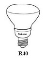
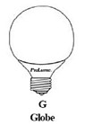
Bulb Shapes
Singapore commonly used bulb shape & base is highlighted in bold font. |
|
|
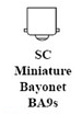
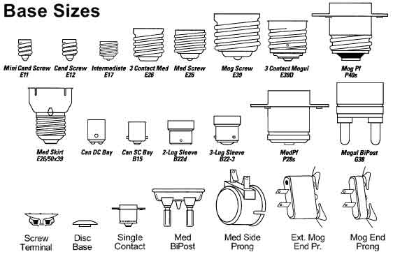
Base Sizes
Singapore commonly used bulb shape & base is highlighted in bold font. |
 |
|
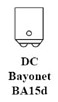
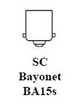
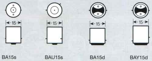
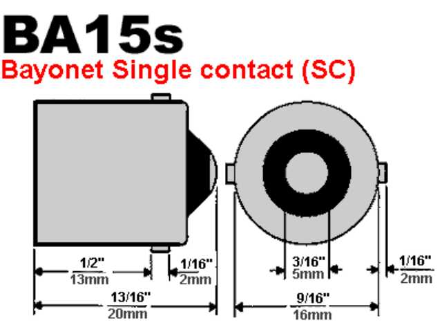
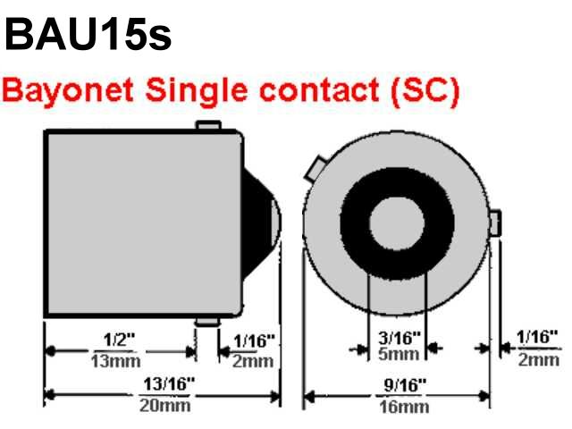
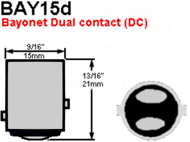
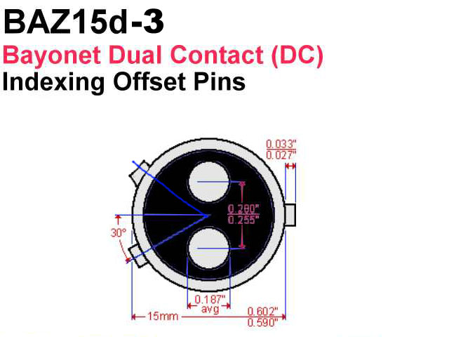
BA15s BAU15s BA15d BAY15d
BAZ15d BAZ15d-3
SBC B15d BC B22d Singapore commonly used bulb shape & base is highlighted in bold font. |
|
|
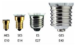
MES E10 SES E14 ES E27 GES E40 Singapore commonly used bulb shape & base is highlighted in bold font. |
 |
|
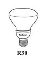
| A-Shape |  |
|
| Chandelier |  |
|
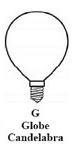
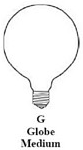
| Globe |  |
|
| GU10 |  |
|
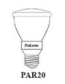
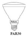
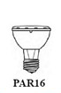
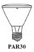
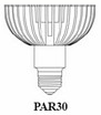
| PAR30 |  |
|
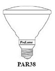
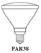
| PAR38 |  |
|
| R20 |  |
|
G4 GY6_35 |
 |
|
| MR16 G10 |  |
|
| MR16 G5.3 |   |
|
|
||


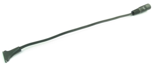
Useful accessories for lamp installation
|
||
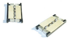
1) ETON Connectors
|
Reference:
Graphics in this webpage are re-compiled from the following website:
– http://www.superiorlighting.com/Light_Bulb_Shape_and_Size_Reference_Guide_s/218.htm
– http://www.ledlight.com/LED-Information.aspx
– http://www.nzlightingltd.co.nz/Useful+Hints/Choosing+a+Bulb.html
– http://www.customdynamics.com/bulb_identification_help.htm
Keyword: Lamps, LED, Fluorescent, Singapore, Energy saving, Bulb shape and base


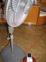
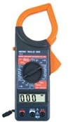 A
picture if the clamp-ammeter for measuring the current flowing through
your electrical appliances. Clamp the live or neutral wire of your
electrical cable to measure the current flowing.
A
picture if the clamp-ammeter for measuring the current flowing through
your electrical appliances. Clamp the live or neutral wire of your
electrical cable to measure the current flowing. 


 Front
Front Back
Back


 RC filter, the simplest low pass filter.
 Another way of looking at the same RC filter.
  A capacitor as a low pass filter.
 RC filter, the simplest high pass filter.


 A
phone small enough to carry around.
A
phone small enough to carry around.
 Mobile
phone as thin as biscuit.
Mobile
phone as thin as biscuit.


 Rework Station


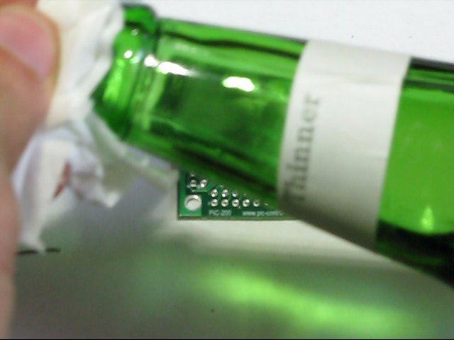

 Alcohol
& thinner has a lower flash point, and catch fire easily. You have to be
extremely in handling and storing these flammable chemical. Do not store or
work on the chemical near electrical appliances, hot area or things that can
cause spark. Keep your windows open to allow air to circulate while working
with these chemical. They may cause headache, dizziness and uncomfortable
when inhaled.
Alcohol
& thinner has a lower flash point, and catch fire easily. You have to be
extremely in handling and storing these flammable chemical. Do not store or
work on the chemical near electrical appliances, hot area or things that can
cause spark. Keep your windows open to allow air to circulate while working
with these chemical. They may cause headache, dizziness and uncomfortable
when inhaled.


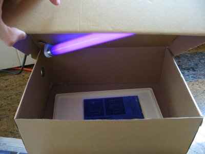

 ultra-violet exposure


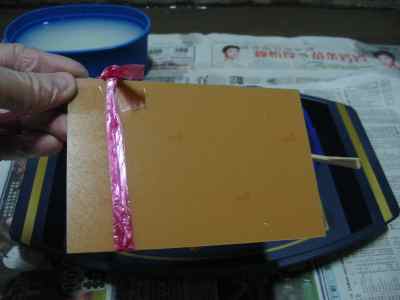
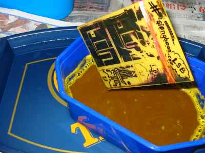
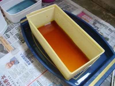
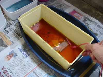
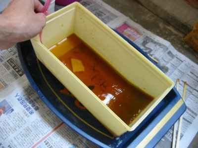
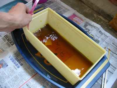
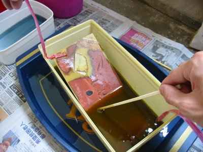
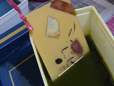
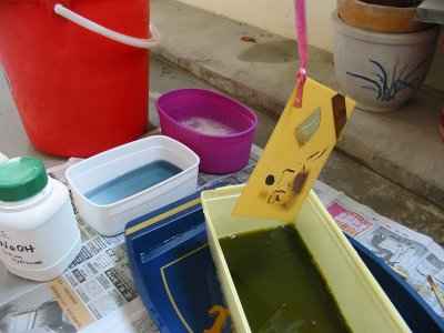
 When mixing
NaOH to water, heat will be produce. Stir the water solution constantly
while adding in NaOH slowly.
When mixing
NaOH to water, heat will be produce. Stir the water solution constantly
while adding in NaOH slowly.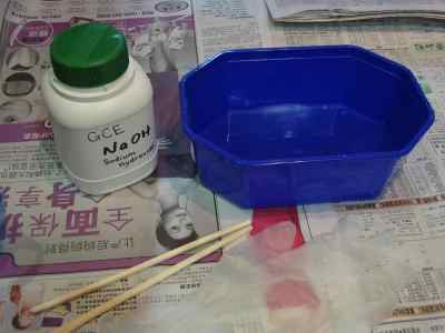


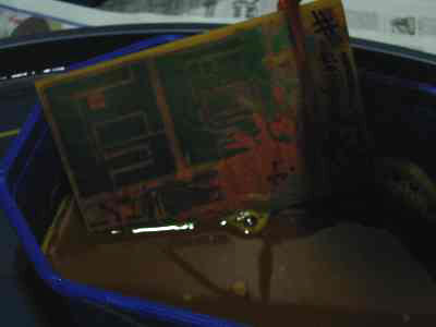
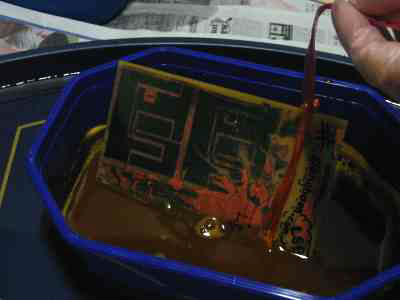
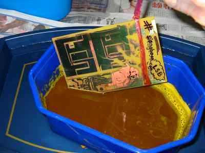


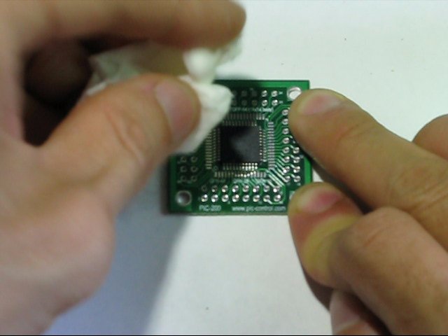
 tinned PCB board.


 Standby power is 1.2W
  Even if the loud door bell ring is activated, the consumption still remains at 1.2W.
  The door bell transmitter outside the door is using a battery.


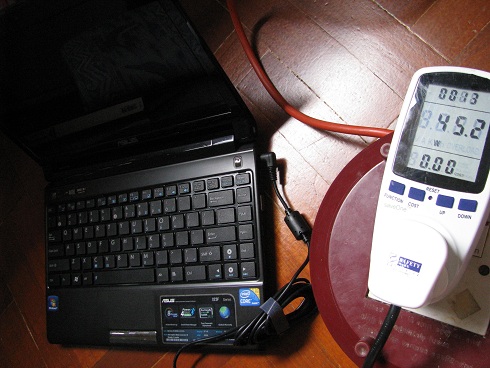

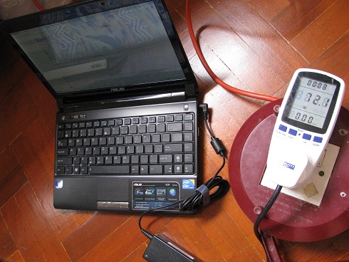

 The laptop was shutdown, and the power consumption drop back to 0.328A, 0.69PF. Should be about 45W.


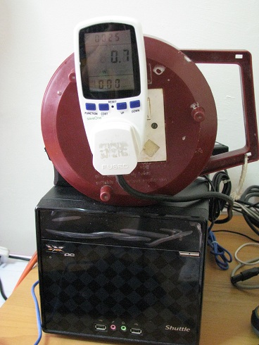
 Power consumption during standby with mini PC switched off.


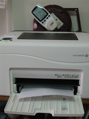
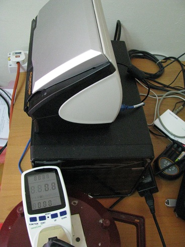
 Printer on standby 11.5W to 750W
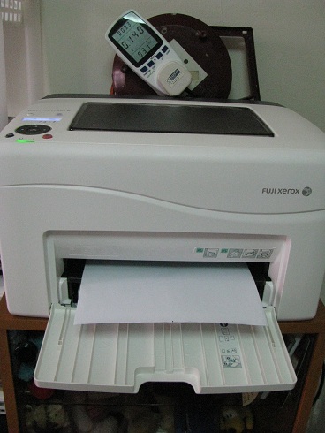
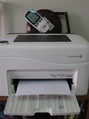
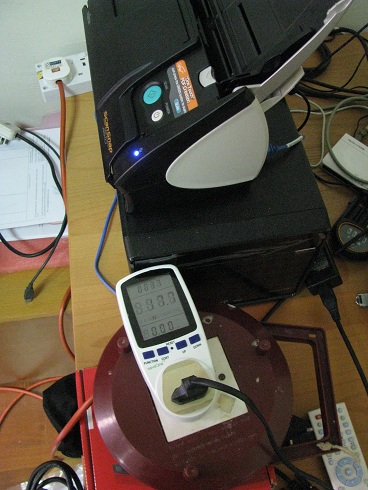
 Printer reaching its peak 776.1W.
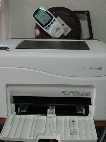


