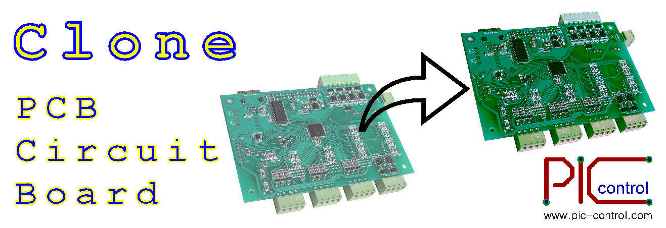
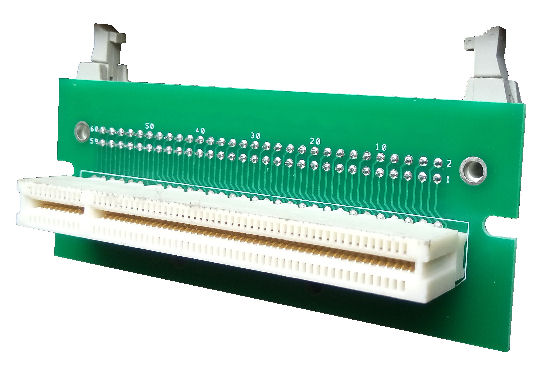
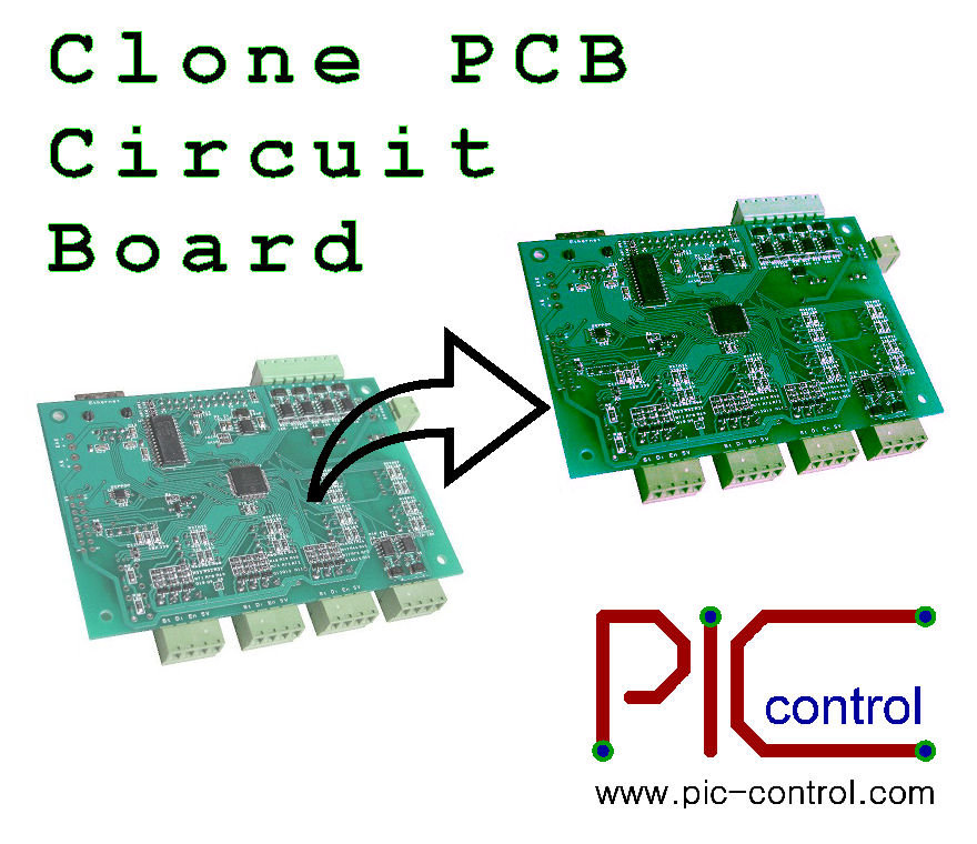
Stacking PCB Board IC Tray Design

PCB reflow tray for testing IC chipsQFN 3x3mm reflow tray for IC chip using PCB boards

Reflow Tray for IC Chip Baking Temperature Testing

PCB tray design for temporary IC chip baking testing. Suitable for testing IC chip under reflow soldering temperature.

There is a limit of PCB tray reuse. PCB tray is not suitable for repetitive usage.

Features

  • For QFN IC chips
  • Holder on board for 280pcs
  • Stacking screw/nut design
  • A top cover to protect IC chip from blowing away.

Stackable Tray Design

The baking IC Tray is designed to be stackable with a cover on the top.

stacking IC Tray PCB boards with covering  

Stacking IC Tray PCB boards

Contact PIC-CONTROL for your custom reflow tray for IC chips.


Connector Adapter PCB Board

IDC connector to terminal block wires output connector (adapter PCB board)Spring release terminal block for wires output. IDC to wires converter board.

IDC to Spring-cage Wire Connector Adapter Board

This adapter board helps convert your ribbon cables IDC connector to individual wire terminal connection. The wire output is inserted via the spring release terminal connector. Simply push the lever with a sharp tool (for example a screwdriver), insert your wire and then release the lever. Quick and simply for individual pin wire connection.

Features

  • 60 pins IDC Connector with a quick connector release lever.
  • 4 pins 3.81mm pluggable terminal vertical connector. (power input connector)
  • 6 blocks of 10 pins Spring-cage wire connectors.
  • Design for DIN rail bracket mounting.

DIN rail hole mounting for IDC and wire terminal block connectorsSpring cage connector to lever release IDC connector converter board

Custom Connector Converter PCB Board

For other custom PCB board design for connector conversion adapter board, please provide us with further details.

Contact PIC-CONTROL for Custom Connector Converter DIN rail mounted adapter board.

DIN 41612 to IDC connector adapter PCB board


Card Edge PCI to IDC Connector Adapter

Card Edge connector adapter board

PCI to IDC Connector Adapter Board

Adapter board is designed for Card Edge board.

This adapter is custom design to convert 120pins PCI connector for access via a 60pins IDC connector.

Card edge PCI connector adapter PCB

Finger Connection Edge Pins

Card edge connector is designed to fit PCB edge finger connection pins. PCB board is typically 1.6mm in thickness.

The pins design is embedded on the PCB itself (board to board connection), saving you the need to buy and install a connector on the PCB board. This is much more cost-effective solution.

The PCB card is easy to plug in and out, making it suitable for hot-swap and mass test connection.

Typical Application

  • Mass testing of assembled PCB.
  • Extension of board functionality.
  • General purpose I/O processing board.
  • Hotswap electrical connection.

Card Edge PCB board connection pins

Finger connector pins on card edge PCB board

PCI connector pins on the board edge

Custom Card Edge Adaptor Board

PCI to IDC connector adapter for card edge PCB board

Contact PIC-CONTROL for your custom Card Edge PCB board design and fabrication.

We design for any type of card edge board connection.

Light Indicator Panel Board

Light Indicator Panel Board

Custom made indicator panel board monitor your electrical devices status.

Can be used for 12V or 24V devices.

Monitoring the status of your sensor input or output actuators.


12V 24V LED Indicator Panel BoardLight Indicator Panel for monitoring of electrical status

Board can be design for easy DIN rail mounting.

Other Electrical Box Product Solution

Contact PIC-CONTROL for more information
or check up our custom electronic solution website for more information.


PCB Standoff

PCB Standoff

  • Brass (most common)
  • Plated Steel
  • Nylon

brass PCB standoff     Nylon PCB standoff

These PCB standoffs available in brass, steel or nylon material. The threaded ends are for typically M3 and M4 screw size. One side can be a male thread and the other end a female thread. Both end female thread is also quite common. The standoff length is usually in millimetres (even number, example: 4mm, 6mm, 8mm, 10mm, 12mm, etc…

Nylon is light in weight and has a non-magnetic property like brass. Screws and nuts are also available.

PCB Standoff Base

The PCB standoff base can be secured underneath the PCB board and provide your board with the support. This can lift up the PCB board so that the bottom side will not be touching the table surface. This is useful especially if the table is metallic or there are many metal parts laying around. A simple standoff base will reduce the chance of accidental short-circuit, without having to spend time and money on a casing.

These bases come with a double sided adhesive tape below. It allows you to secure it onto a casing or a surface plate easily.

Adhesive Standoff Base with M3 nut thread for securing to PCB board

PCb Standoff Base (Black color, M3)     PCB Standoff Base illustration

Screwless Standoff Base

Nylon PCB Standoff base for hole size 4mm         PCB Standoff Base illustration     Nylon PCB Standoff base

背胶固定座 PCB M3

SMD PCB Standoff / Spacer (surface mount)

https://www.dmtl.co.uk/product-series/smd-pcb-spacers-standoffs-power-elements-for-high-current-applications-smt-terminal-blocks

PCB Board Fabrication

Introduction to PCB Board Fabrication

When submitting your design to a PCB fabrication factory, it is easier to submit the universal Gerber file format. Some factories do accept specific format from a particular software. You can easily generate the Gerber format of your PCB layout design through any PCB design software. Please indicate the following when submitting your PCB Gerber files to your PCB fabrication factory,

  • PCB Fabrication Specification
  • Quantity Required
  • PCB board size (if Gerber files is not available yet)

The information will help the fabrication house to reply you with a quotation promptly. The next few section provide the details that you need to know before approaching the PCB fabrication factory.

PCB Specification Specification

The PCB fabrication specification tells us how you would like your PCB board to be produced. For simple electronic circuit (2 layer board), we will usually recommend the following commonly used industrial grade PCB specification,

PCB specification:
FR-4, 1.6mm, 2L, 1 oz copper, Green Mask, White Silkscreen, HASL

If you would like to find out more details about the PCB specification above, check out this PCB fabrication specification page.

Quantity Required

PCB fabrication production quantity can be as low as 1 piece. As a general guide, the cost of each PCB board reduces as the quantity increase. There are works involve in setting up the machinery and process for the board production of a PCB design. You can specify the exact quantity that you need for your PCB board.

For the purpose of circuit prototyping, you may only need 1 or 2 pieces for testing. Our recommendation is to fabricate 5 pieces to cater for unforeseen rework or modification. The total cost of the fabrication job between 1-5pcs is not very significant.

A typical recommended quantity for PCB production, assembly work would be 5pcs, 10pcs, 25pcs, 50pcs, 100pcs, etc… These quantities tend to be more cost effective, in the various stage of the production process.

PCB Board Size

PCB board size is directly related to the material used. The cost for each PCB board is directly related to the cost. A bigger board will cost more than a smaller board.

Keeping the board small can help to reduce production cost and future cost (like product shipping, storage, etc…). For mass quantity production, it will make economical sense to design the board smaller.

Designing smaller PCB board can also mean a higher cost in PCB design. More thoughts and time will be needed to layout the components and traces onto a smaller board space. This higher cost in designing the PCB is usually negligible for high volume production.

Want to fabricate your PCB board?

If you have your PCB board design with your Gerber production files ready, check out our PCB fabrication service.

We are offering a standard pricing for the fabrication of your PCB prototype.

Want to design an electronic product?

PIC-CONTROL helps our client to custom design electronic product for their business. We focus on the engineering aspect providing our customers with a unique custom electronic solution. Check out these other pages for our Electronic Design or PCB Design Services.

Other Services

We provide electronic circuit assembly service and other electronic manufacturing services too. Check them out.

Reduce Electrical Wiring for DB Box

Electrical wiring may seem to be a simple job, the scale of the work is typically massive. The wiring job for a home or an office can take days to complete. Any slight wiring improvement can often help save a lot of time and cost.

No More Messy Cables Wiring !!!
Electrical wiring in a mess.


Print your wiring onto a PCB (Print Circuit Board) to

  • reduce Size and Weight.
  • reduce Assembly and the number of Connection.
  • reduce the Wires materials, components.
  • easier to handle.
  • reduce Production Time.
  • reduce Man-hours manpower.
  • reduce your Production Cost.

Distribution Box (Electrical DB Box)

Connecting a wire termination in the DB box may take less than a minute of work. When connecting thousands of wire termination, the work can take days to complete. Reduce and simplify wiring work can significantly improve your efficiency and man-hour cost.

Wiring in the DB box forms the connections between termination to achieve a function. If your wiring function is consistent and repetitive, you may like to consider fabricating a PCB board to reduce the massive connection work. Not only can it save you time in your man-hour, but your wiring will also be neater, saving your significant cost in the long run.

Wiring board for electrical wiring connection (front).Wiring board for electrical wiring connection (back).

Reduce electrical wiring connection in a DB box using PCB board.

PCB board reduce wiring for electrical box     Elco wiring board example.


A simple board from Elco to help reduce distribution box wiring connection.

Reduce Wiring Cost

A significant of the project cost can be due to the massive amount of wiring laid across a distance of 100m or more. If your cable is only used for signalling, and not for the purpose of delivering power, there is a chance that your cable can be further reduced, saving you on the cabling cost.

PCB drawing for simplify electrical wiring connection.     PCB wiring drawing for electrical panel

Send us your electrical wiring/cabling problem that you have onsite. We can help you assess a solution to help you improve your efficiency and reduce your costing.

Contact PIC-CONTROL now.

Check out other related products which is design to help you reduce your wiring work in an electrical box.
Alarm Monitoring Panel Interface Board
LED Indicator Light Panel Board for monitoring the status of your 12V 24V electrical system.

Check out our home page, PIC-CONTROL, your electronic design and manufacturing provider in Singapore.

PCB Design – Tips on laying out a good PCB board

Designing electronic circuit is only the beginning of translating an idea into a physical product. The next important step is to translate your schematic design into a layout on a PCB board. This is known as PCB circuit design. A PCB board provides the platform to hold electronic components (IC chip, resistors, capacitors, inductors, etc…) and enable their connection (known as PCB traces). It is also the main means to replicate the connections for mass production purpose. Most PCB boards are green in colour (we call it green coloured mask).

PCB circuit board design and layout service in Singapore

For small quantity production or simple electronic circuit prototype, PCB circuit design is usually not required. This is because designing the layout for the circuit can take up engineering effort. A typical simple circuit can take from 3 to 7 days to design and layout. This is a fixed cost prior to your production. Good news is that you only need to do it once. With this PCB blueprint (commonly refer to as Gerber files) you can reproduce as many PCB board as you like. For larger mass production quantity, the circuit design and layout cost is usually insignificant compare to the cost of each board. If you are only producing a few pieces of a simple electronic design for prototype testing purpose, this engineering effort may not be worth the value. It maybe cheaper to use a prototyping board instead to build and test your design.

PCB Design

The PCB circuit design is a combination of knowledge in electronic and user interface art. Engineering know-how to ensure the circuit works without issues, and also to design it in a simple manner such that the people using the circuit board product can easily handling it.

Engineering Know-How

Design PCB board requires a certain skill set. Besides the basic knowledge of electronic, a good foundation in the area of RF (Radio Frequency) is preferred. It may seem odd so some. What is RF going to do with PCB design? Wireless and PCB is a different topic, aren’t they? No. In fact, they are very much closely related. Knowledge of RF provides us with a strong understanding of how electronic circuit behaves under high-frequency condition. It is also related to how the electronic components and traces should be layout in order to keep the signal integrity within an acceptable tolerance, keeping the noise (unwanted signal) minimum. This is especially important when your electronic design contains sensitive analogue circuit, high-speed digital circuit or RF circuits. There rules to follow to ensure that the electronic signal maintains its integrity.

General rules that you can follow

  • Learn to identify and categorises circuit trace. For example Power, Digital, Analog, RF traces.
  • Design the PCB layout from left to right, starting from the power, input, and finally to the output.
  • High power circuit modules, input or output should be located closely to one another to shorten the trace. This not only reduces board space it also minimise temperature rise.
  • Power trace should be board enough to conduct the current without generating significant heat. As far as possible VCC & GND trace should be routed in a pair close to one another. This is to minimise the open (or known as loops) between the VCC & GND trace. The same applies to other types of traces. Power distribution is better to be in a star configuration. This is especially if the circuit module is very noise or high current. A delicate trace directly from the power source to the noisy circuit helps isolate it from the rest of the circuit.
  • For digital data trace, if the data is of high-speed type, try to route it closely to a digital GND. Data rate >10Khz, you should start to consider proper digital trace routing.
  • Analog signal trace, route it close to its GND trace as a pair. Leave sufficient gap away from high power or high-frequency digital trace.
  • Group related circuit module tightly together to minimise the length and number of trace between circuit modules.
  • Digital circuit and Analog circuit should have their own GND route. Should not mix.
  • Before starting your 2 layer PCB board design, decide if the top or bottom layer should take on a horizontal or vertical trace. For example, if top layer traces are drawn horizontally, then the bottom trace should be vertical. This will help make tight routing simpler.
  • For those un-used PCB board surface, use GND copper pour near circuit that generates more heat (for example, copper pour near power circuit). The copper pour acts as a heat sink for the heat. Also, you may like to copper pour over the area that contains sensitive analogue circuitry.

Design for Usability and Maintenance

  • For side entry connector, if possible, consolidate them on one side so that the installation space needed for wiring can be minimised.
  • A component with polarity +/- should have silkscreen indicating the component’s polarity. (Diode, LED, IC, Capacitor, etc…)
  • If space permit, print the component value next to the component.
  • Design surface mount component. It saves space and is easier to assemble compared to through hole components.

Quick PCB Design Checklist before sending for PCB fabrication

Here is a quick checklist to go through after you design the PCB board. This check list wraps up the additional details completing your PCB board design.

  • Mounting hole for PCB board. (usually 3.2mm hole for M3 screw size)
  • Ensure the input and output port connector is properly labelled for the user.
    for example:

    • Pwr In, + 12V –
    • LED indicator, RUN, COMM, ERROR
    • Switch and Jumper pins.
    • Input-Output Connector, Port01, Port02, +/-
    • Ethernet, RS232, RS485
  • Label for the name, product code and version for the PCB design.
    for example:
    USB I/O Controller
    PIC-304 ver1.0
    Made In Singapore
  • Labelling of components and its value on the PCB board to aid in the production.
  • Setup some test pin or pad for production testing process, verifying for the valid voltage.
    • check for power input voltage
    • check for regulated voltage
    • check for analogue circuit voltages

Typical PCB material specification

Before any PCB fabrication is started, you will need to specify the type of material to be used for your PCB. There are many types of material specification. For a typical industrial grade PCB material, it is recommended to use the commonly available,
Typical PCB specification: FR4, 1.6mm, 2L, 1oz copper, Green Mask, White Silk, HASL.

  • FR4 is the fiberglass material PCB board. There are also other type of PCB board materials. Some cheaper cost, lower durability. Some are used for specific high frequency application, which can be more expensive. FR4 is the most commonly available material and good enough for most application.
  • 1.6mm is a common PCB thickness. Most components, connectors (RJ45, DB9) footprint uses this standard thickness.
  • 2L means 2 layer PCB board.
  • 1oz copper is the thickness of the copper layer. 1oz is good enough for most application. If your trace is small and current flowing through is high, you may like to increase it to 2oz or more to minimise the heat that can be generated from the trace.
  • Green Mask, the color of the mask which is also the PCB board color. Some of the commonly used color are blue, red, black, white, etc… Green mask is still the best, trace is more visible.
  • White Silk, specify the color of the silkscreen printing use for all the components and connectors labeling.
  • HASL (Hot Air Solder Leveling) specify the type of plating/costing to the exposed copper pad. Without the coating, it means that the expose surface will be bare copper. Leaving the copper surface expose to the air can result in oxidation on the surface. Once the pad is oxidation, soldering will become difficult. Even if it can be soldered, the soldered joint will not be good. This may cause intermediate issue when your circuit board is operating. There are many type of finishing. Gold plating is one of the options. A minimum plating thickness is required to minimise oxidation. Gold is expensive and is typically not needed. HASL is simply a coating of solder on the copper pad to prevent it from oxidation. It is a common cost effective method.

You can also check out more details of this recommended PCB specification on this page.

These are the basic things you should take note when designing your own electronic PCB circuit. If you need further assistance regarding PCB design or electronic circuit design, feel free to contact PIC-CONTROL using the message form on the right side bar of this page.

Copy PCB


Copy PCB in Singapore


Clone PCB Circuit Board

Copies of a PIC-250 LED PCB boards


You have a physical electronic circuit board on-hand but do not have the circuit design files?

You do not have any PCB Gerber drawings files, for your PCB production and circuit assembly.

You want to reproduce the circuit board (PCB), but you do not have the blueprint, or the blueprint is missing.

Send us a photo of your electronic circuit board that you want to copy. We can assess the PCB copying for you.

Please send in:

  • Photos of your circuit board.
  • Description of the board’s application.
  • Reason for copying the board.

Contact us today for your PCB enquiry.

Looking for an engineering service to copy your PCB board or electronic circuit locally in Singapore?

PCB Cloning Service

PCB cloning service enables you to replicate the same copy of electronic circuit board that you want. For a simple electronic circuit, copying the PCB circuit board is not too difficult. If the circuit involves intelligent controller, cloning should be the last resort that you should opt for as a solution for your engineering or business challenge.

Copy PCB service in Singapore

Copy PCB for Simple Electronic Circuit

PCB cloning for a simple circuit is normally not too difficult. The following is a typical procedure in the copying of PCB board,

  1. Evaluate all the Components on the PCB board.
  2. Trace out the component connection.
  3. Document the schematic of the connection trace.
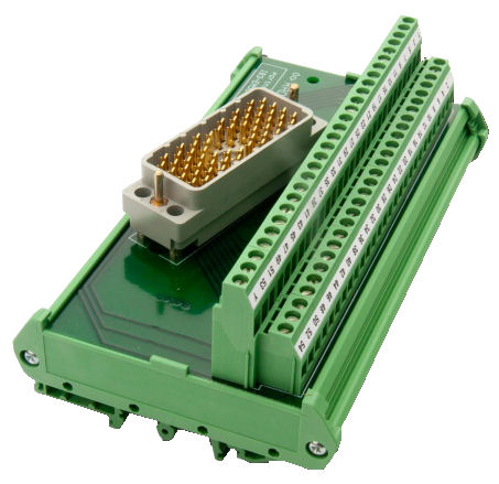
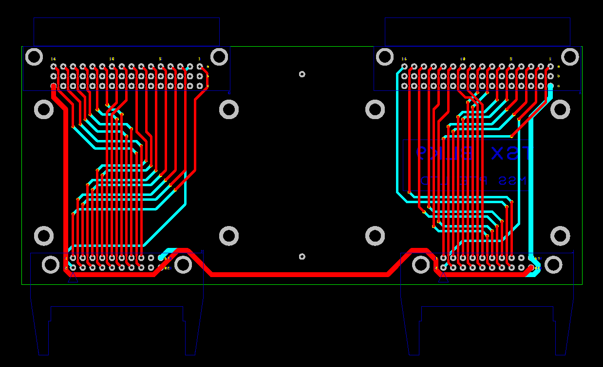
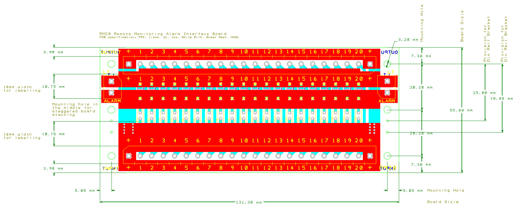
  4. Draft a new PCB layout.
  5. Mass production for the copied PCB electronic circuit.
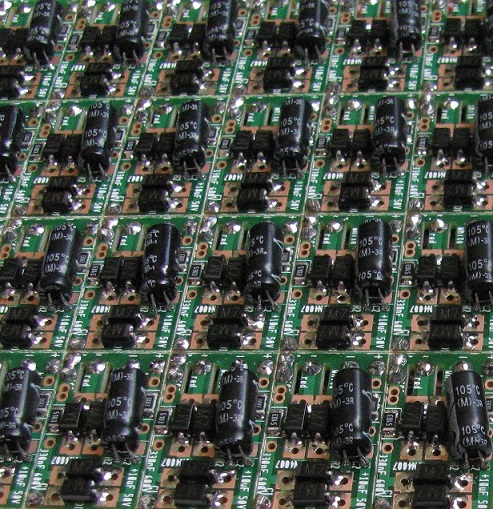
Copies of PIC-018 production PCB boards   Assembled copies of PIC-018 LED driver circuit boards.

Evaluate Components

All the components on the PCB have to be evaluated. This step is the determining factor in classifying the cloning work to be simple or complex.

Passive components like the resistors, capacitors and inductors are usually simple to source and purchased.

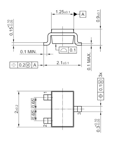
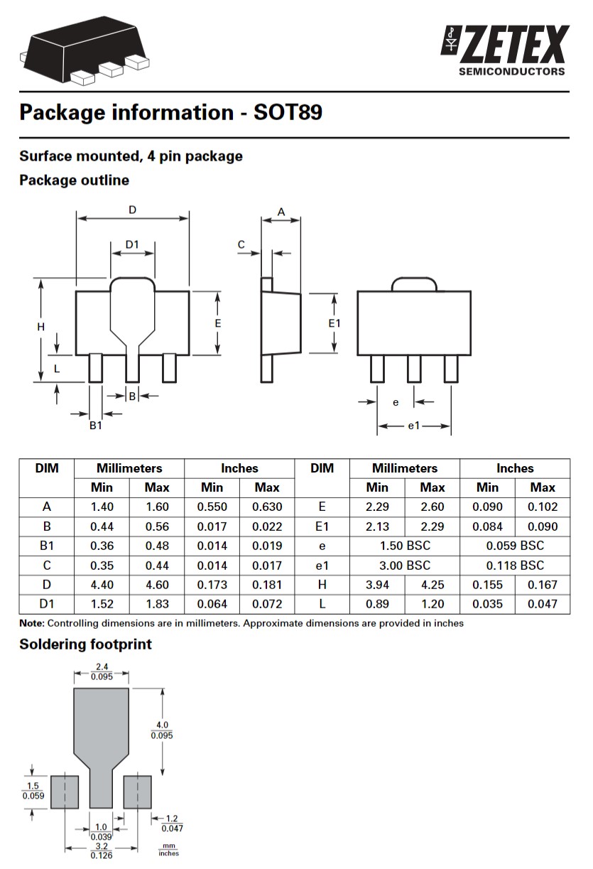
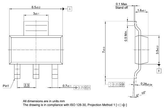
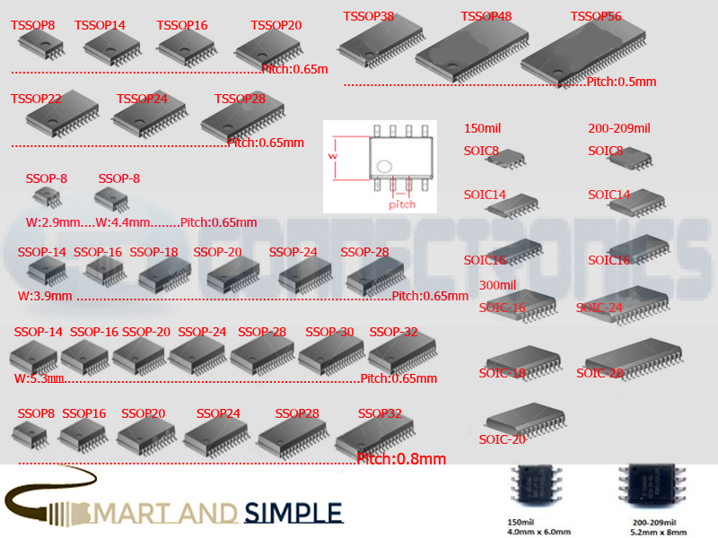
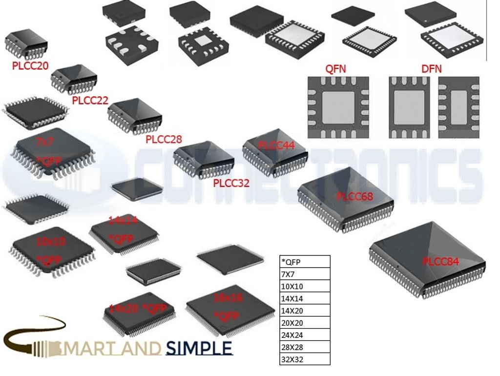
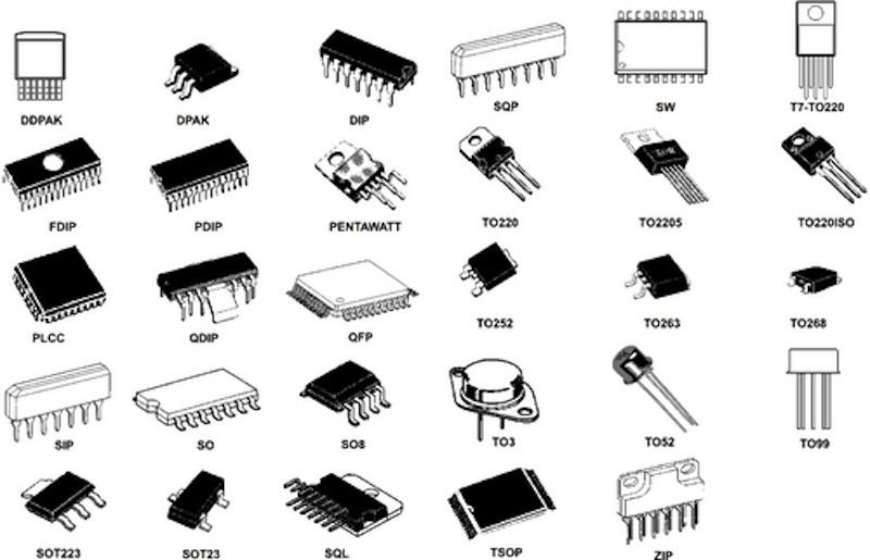
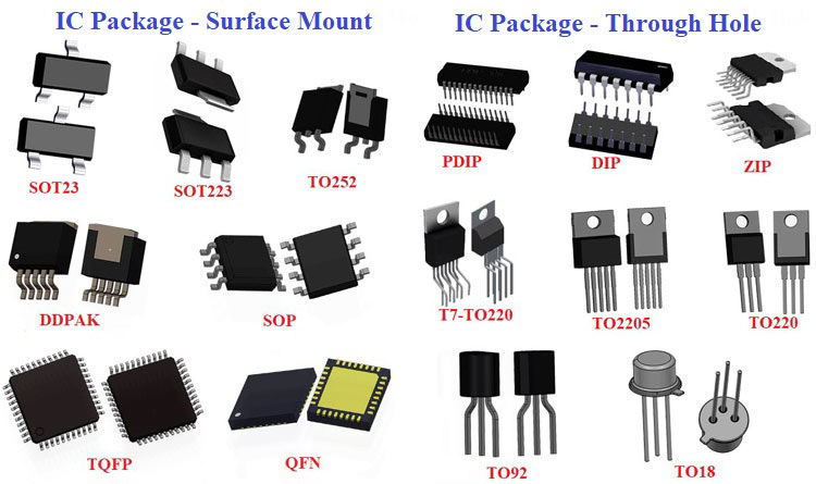
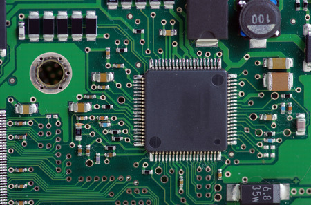
Active components like transistors, diodes or IC chip may be harder to source for the exact part number. This is especially if the component’s package size is small. Part number may not be laser engraved on the component’s packaging. Usually, a marking code (normally about 2 to 5 alphanumeric code) is represented on the top or bottom of the package instead of the full part number. Using marking codes to source for the component part number can sometimes be quite challenging, taking a very long time.

For cases where a component cannot be determined, the next step will be to determine the component from the schematic being traced out from the components’ trace connection. An experienced electronic design engineer should be able to tell the classification of the component, and hence able to deduce the exact part number. The component may also be narrowed down to a close compatible alternative.

In the worst scenario where the alternative replaceable component is not possible, the electronic designer will have to base on the specification and function of the board to re-design a portion of the circuit to replicate the function in your original circuit. This is also why it is important to provide our design engineer with the details of your circuit functionality. By knowing how your circuit function we are able to recover the function by using alternative design.

For detected IC chip that is a microcontroller or memory components, the difficulty level can become much higher. Besides the hardware circuit evaluation, the engineer also has to dig deeper into the firmware (source code). It is rare where the firmware on the chip is not protected, but there is still a chance that it can be copied out.

Cloning Microcontroller IC chips

Cloning of microcontroller chip involved in reading out the machine codes (firmware or program) from the internal EEPROM memory. Reading the microchip may not be successful if the manufacturer locked up the EEPROM to protect their codes from being copied.

Common microcontroller chips to clone/copy

  • Microchip microcontroller chip
  • ATMEL microcontroller chip
  • Arduino

Click here for more information on how we can help you to clone your microcontroller chip.

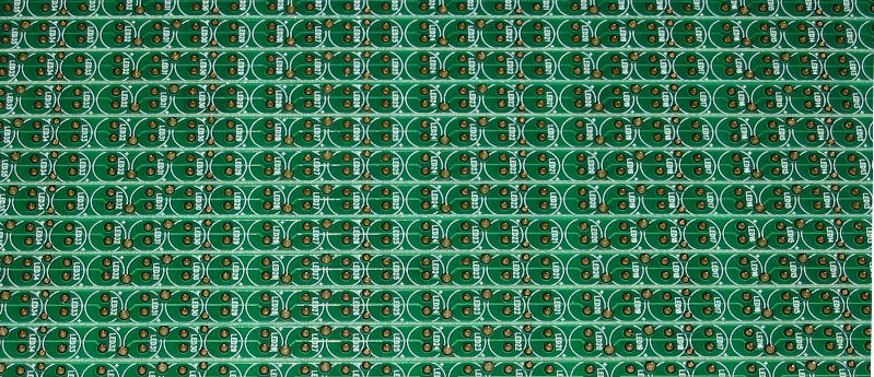
Tracing Out the Components Connection

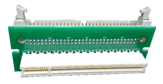
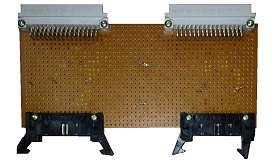
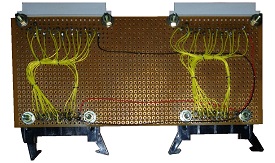
Tracing out the component is a tedious process. For single layer PCB board, tracing the connection is quite simple. Visual tracing of the components is enough to trace the connection.

Double layer board is not as simple, but it is still a possible task. Tracing of the component connection may be more difficult using visual when the via (connection between the top and bottom copper layer) is being hidden under a component. The connection can be evaluated with a multimeter to check for connectivity.

Multilayer board is almost near to impossible to trace if the board contains many components. There will also be buried via which cannot be easily detected visually. In some cases, X-Ray is needed for the trace. Multilayer board makes connection tracing very challenging.

Consider Development of a New Board

PCB cloning involving a controller will be more time consuming than designing the circuit from scratch. This also means that the cost will be much higher. For copying circuit involving a controller on the circuit board, you should consider seeking an electronic engineer or an electronic design company to evaluation the development of the electronic circuit that you need. Get a quotation to understand the cost to develop the solution from scratch instead of copying it.

In some situation, electronic circuit development work can also be very costly. This is especially true for designed circuit deployed for a complex application. In this case, you will probably have no other choice but to copy PCB board through a local PCB cloning service provider.

The replicating process for a complex electronic circuit is also known as reverse engineering. Reverse engineering is more like a work of art. The work requires the engineering brain of an experienced electronic design engineer, and also the creative mind of a detective. The process requires a lot of thinking and searching. It is like trying to solve a puzzle. You may like to visit this page for reverse engineering of an electronic circuit board. Or check out his web page for our shared resource for reverse engineering work.

Rows of PIC-250 LED PCB Boards

Contact PIC-CONTROL for PCB Copying Service

Click here to find out more about the workflow for copying your circuit board.

Copying PCB is not a cheap solution especially if your board is complex. For a board that contains a microcontroller IC chip, it is considered a complex board. For the complex board, copying may not be as simple as it sounds. There is a fairly high chance that it needs a reverse engineering process instead. If a new equipment is not expensive, you should seriously consider changing the whole equipment.

For a simple board (without a microcontroller or microprocessor), there is a much higher chance of copying directly.

If you would like to seek consultation regarding electronic circuit copying or cloning, feel free to contact PIC-CONTROL.

The followings are what we need from our client,

  1. The reason that you want to copy the board.
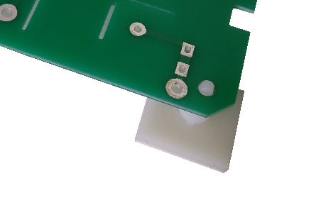
  2. Photos of the PCB board that you want to copy.
  3. The description of the board use and application.

Send in your enquiry to our sales email address.

We may reject your enquiry if the background information of your project is insufficient.


Clone PCB Circuit Board

Categories PCB

Manual Wiring on Prototyping Circuit Board, Electronic Design

Prototyping boards allows electronic components to be manually soldered and secure neatly onto a board platform. Compare to plugging the electronics component onto a temporary breadboard, a prototyping board offers a better reliability. It is robust enough for a one-time project deployment. There are many types of prototyping board to suit your prototyping needs.

Benefits of manually wired prototype circuit

  • Design changes flexibility during the development phase of the first prototype.
  • Less initial investment for proof of concept.
  • PCB Design drawing need not be drawn first.

Disadvantages

  • A Slow and Expensive method if your production quantity is large. (eg. > 10pcs)
  • Not suitable for fine pitch IC chips and components.
  • Limited choice of connectors.


Some samples of designed electronic prototype circuit manually wired on a prototyping circuit board.

DC Motor Controller

DC Motor Controller Sensor Input Interface Board

Circuit layout and manually wired on an FR2 prototyping board.

RS232 I/O Controller

RS232 I/O Controller RS232 I/O Controller

Circuit illustrating electronic circuit assembly using an FR2 prototyping board. The back side of the PCB showing point to point wire wrapping wire soldering. Soldering point to point is simple, and make good electrical connection. The connection is soldered onto the pin and will not easily disconnect.

LED Backlight Driver Circuit

LED Backlight Driver Circuit Board LED Backlight Driver Circuit Board

Alarm Notification RS485 Communication Prototype

Input Alert Notification RS485 Communication  Input Alert Notification RS485 Communication

Neat custom component layout with the point to point soldering using wire wrap wires on an FR4 prototyping board. The FR4 board prototype boards have rows/columns of holes which are inter-connection on both sides of the board. The top of the PCB is neatly mounted with through hole components, while the back of the PCB has the electronic connection with the point to point soldering.

Load Cell Electronic Reader Circuit (Digital Weighting Scale)

Load Cell Electronic Reader Circuit 1 Load Cell Electronic Reader Circuit 1
Load Cell Electronic Reader Circuit 2 Load Cell Electronic Reader Circuit 2

PIC-210 Prototyping Board (front)

PIC-210 Prototyping Board (back)

This is partial PCB and manual wiring connection on the PIC-210 prototyping board. The prototyping board is partially pre-connected to the standard connection, saving you time to manually connect them point by point while providing you with the flexibility of wiring for your electronic circuit prototype.

Visit the prototyping page for more information about PIC-210 prototyping board.

Magnetic Field Sensor Array

Magnetic Field Sensor Controller  Manual wiring of an electronic prototype design can allow you to have tight component placement, which help keeps your board space small.
Magnetic Field Sensor Array (front) Magnetic Field Sensor Array (back)

RFID Card Key Reader Prototype

RFID Card Key Reader (front) RFID Card Key Reader (back)
RFID Card Key Reader (front) RFID Card Key Reader (front)

This is another prototyping board for microchip 6 to 8pins microcontroller series. Build up your prototype and customise the design by doing manual point to point wiring connection.

Visit the prototyping page for more information about PIC-211 mini prototyping board.