PCB fabrication specification tells us the details about the PCB board that we want. It is important to understand the specification just a little more, which helps you to tell the PCB manufacturers the type of PCB board that you need. There is numerous PCB fabrication specification which describes a PCB product. Studying everything may not be necessary and can be overwhelming for beginners, especially when you only need a simple PCB board. The following present the most common specification used in PCB board manufacturing.
Typical PCB Fabrication Specification:
FR-4, 1.6mm, 2L, 1 oz copper, Green Mask, White Silkscreen, HASL
(Approximated PCB weight about 0.004g/mm²)
This is also what we recommend for most of our customer’s PCB board product. We will talk more details about this typical PCB fabrication specification.
FR-4 (Standard PCB material)
The standard PCB material used is commonly FR-4. It is a durable PCB material suitable for most type of application. It is a Flame Retardant (which gives its name FR grade 4) glass reinforced epoxy laminate material, which is resistance to flame, good strength, and is resistance to water. It is a very common board material used for PCB fabrication.
There are many other types of materials available for PCB fabrication. We do not recommend other materials other than FR-4, unless your design requires the specific specification, or is suitable for your situation. There are advantages and disadvantages for each of the material. In most situation, FR-4 will be enough. For your information, the following are the other type of materials available for PCB fabrication.
- G10, G11, FR-1, FR-2, FR-3, FR-4, FR-5 (flame retardant)
- CEM-1, CEM-3, CEM-5 (Composite Epoxy Material)
- Flexible PCB (for tight space, flexible)
- Ceramic, Metal, Aluminum (for high heat generating components)
- Roger (for high-frequency application), RO3000, RO4000
- Polyimide, PTFE, Polytetrafluoroethylene (Teflon)
1.6mm (Standard PCB Board Thickness)
The standard PCB board thickness is 1.6mm. It is a very common PCB board thickness. 1.6mm provides a stronger support for a typical application.
Most through hole mounted components are designed to be mounted onto a 1.6mm PCB board. Components like an RJ45 socket, DB9 connector, etc… are designed for 1.6mm PCB thickness. Most standard enclosures are also designed for 1.6mm PCB board. Using 1.6mm is recommended unless you have a specific reason to use other thickness. Always ensure that your through-hole components can be properly mounted if you are using non-standard PCB thickness 1.6mm.
For small dedicated design, thinner PCB board may be preferred. In extreme cases, proper routing of traces on thin PCB board it can help to improve the signal integrity.
For rare larger size PCB board design, the board may tend to bend or wrap. Care is needed to ensure that there is sufficient support (or mounting holes) to hold the PCB board. It may be necessary to increase the PCB thickness to 2.0mm for a better mechanical strength.
Some of the common PCB thickness can be 0.4mm, 0.6mm, 0.8mm, 1.0mm, 1.2mm, 1.6mm, 2.0mm,
2L (2 Layer PCB)
2L means 2 layers. For the very simple circuit, you may only need a single layer PCB. In most design, you would easily end up with a 2 layer board. The manufacturing process gets complicated as the number of layer increase more than 2 layers. This also means the cost will be higher for a multi-layer board. Unless you have board size constraint or limitation in your electronic design, it is strongly recommended to keep your PCB layout within 2 layers.
While designing a 2 layers board can be more challenging and time-consuming than a multi-layer board, 2 layer board offers the following advantages,
- Lower production cost
- Lower maintenance cost
- Easier to troubleshoot
- Easier to make repair, modification
- Simple
Check out our 2 Layer PCB design article for further details.
1 oz copper (1 oz PCB)
1 oz copper refers to the thickness of the thin copper layer on the top and bottom of the 2 layer PCB board. The etching of this copper layer will form the copper trace that helps connect your electronic circuit IC chips, active and passive components. Traces that carry signal do not carry much current, therefore the copper layer thickness is usually not a concern. 1oz copper will meet most of the electronic circuit application.
For power circuits or high current design, you may need more copper area to conduct the current. If you have enough space on your PCB layout, you can design your trace to be wider. The wider the trace, the more current it can carry without generating obvious heat on the trace. If space is tight for your high current trace, you may like to consider making the copper layer thicker on the PCB board.
There is a number of standard copper oz available.
Common copper oz,
- 0.5 oz
- 1 oz
- 2 oz
1oz is a safe choice. If your circuit carries 2A or more, you may like to consider a 2oz copper. You can use an oz trace resistance calculator to find out the resistance and heat that can be generated from your PCB layout design.
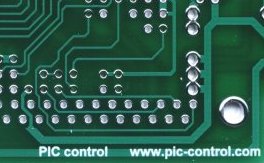
Green Mask (PCB Color)
Green Mask is the main thing that makes most PCB boards look green. The mask is basically a layer of coating to resist against the molten solder.
You can choice colour for your PCB board, other than green. The advantage of doing the typical green mask is that the printed trace can easily be seen, which helps troubleshooting and maintenance work. Green is good for eyes, another reason to use a green mask. Trace that uses white or black colour mask makes it less visible to our eye. If you want to make it slightly tougher for people to study or reverse engineer your board, it can be a good choice.
Typical mask colour are as follows,
 Green (most common)
 Black
Black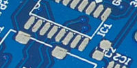 Blue
Blue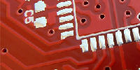 Red
Red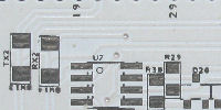 White
White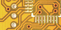 Yellow
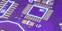 Purple
(click on the image to enlarge)
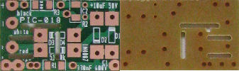
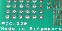
Example of PCB board without any mask and tinned solder
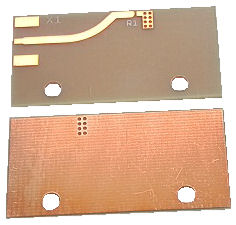 This is how a PCB would look like without any mask coated. You can see the etched copper track on the surface without any solder tinned on the copper.
It usually use in application like RF where any insulation and copper thickness can have a significant effect on the signal result.
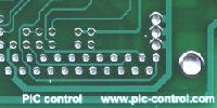
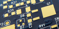
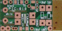
White Silkscreen (PCB silkscreen Label)
White silkscreen is the typical white labelling printed on the PCB board. The labelling allows us to identify the component’s position, orientation, value. It is also commonly used to print out the model product, version and other manufacturing information.
The White colour is a safe colour and is a suitable contrast against a wide variety of PCB base colour (mask colour), except for white base colour.
Common silkscreen colour are,
- White (most common)
- Black
 Yellow
 Red
Red
(click on the image to enlarge)
HASL (PCB Finishing)
HASL stands for Hot Air Solder Leveled. It is a cost effective process to prevent the copper surface (unmask area or the soldering copper pad) from getting oxidise. Copper surface when it is left out in the air without proper storage will get oxidise on the copper surface. The oxidisation will make solder more difficult. Even if soldering is possible, the joint may not be good. HASL basically coat a layer of solder on the surface of the copper pad to prevent the surface from oxidising. HASL is the most widely used and effective finishing.
Other types of finishing for PCB
 HASL, Hot Air Solder Leveled (lead or lead-free)
- Immersion Tin
- Immersion Sliver
 ENIG, Electroless Nickel Immersion Gold
- Electroplated Gold
- Immersion Silver
 OSP, Organic Solderability Preservatives
(click on the image to enlarge)
You can also specify if you would like the boards to be in individual Routed Pieces or in V-Groove Array.
Looking for PCB Fabrication Service?
Now that you have understood more about the PCB fabrication specification, are you ready to manufacture your PCB board design? Check out our PCB fabrication service. If you are looking for our engineer to help you with PCB design, drafting and layout, check out our PCB design service.
Remember the specification for the fabrication of your PCB board when you submit your design to the factory. Bookmark this page now for your future reference.