PCB Design – Tips on laying out a good PCB board

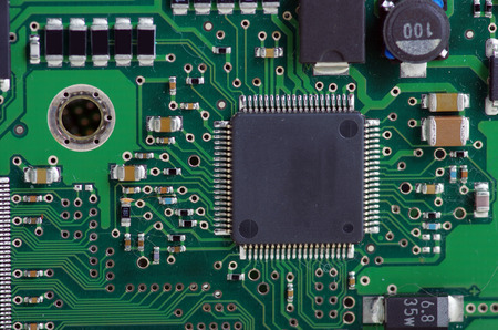
Designing electronic circuit is only the beginning of translating an idea into a physical product. The next important step is to translate your schematic design into a layout on a PCB board. This is known as PCB circuit design. A PCB board provides the platform to hold electronic components (IC chip, resistors, capacitors, inductors, etc…) and enable their connection (known as PCB traces). It is also the main means to replicate the connections for mass production purpose. Most PCB boards are green in colour (we call it green coloured mask).

PCB circuit board design and layout service in Singapore

For small quantity production or simple electronic circuit prototype, PCB circuit design is usually not required. This is because designing the layout for the circuit can take up engineering effort. A typical simple circuit can take from 3 to 7 days to design and layout. This is a fixed cost prior to your production. Good news is that you only need to do it once. With this PCB blueprint (commonly refer to as Gerber files) you can reproduce as many PCB board as you like. For larger mass production quantity, the circuit design and layout cost is usually insignificant compare to the cost of each board. If you are only producing a few pieces of a simple electronic design for prototype testing purpose, this engineering effort may not be worth the value. It maybe cheaper to use a prototyping board instead to build and test your design.

PCB Design

The PCB circuit design is a combination of knowledge in electronic and user interface art. Engineering know-how to ensure the circuit works without issues, and also to design it in a simple manner such that the people using the circuit board product can easily handling it.

Engineering Know-How

Design PCB board requires a certain skill set. Besides the basic knowledge of electronic, a good foundation in the area of RF (Radio Frequency) is preferred. It may seem odd so some. What is RF going to do with PCB design? Wireless and PCB is a different topic, aren’t they? No. In fact, they are very much closely related. Knowledge of RF provides us with a strong understanding of how electronic circuit behaves under high-frequency condition. It is also related to how the electronic components and traces should be layout in order to keep the signal integrity within an acceptable tolerance, keeping the noise (unwanted signal) minimum. This is especially important when your electronic design contains sensitive analogue circuit, high-speed digital circuit or RF circuits. There rules to follow to ensure that the electronic signal maintains its integrity.

General rules that you can follow

  • Learn to identify and categorises circuit trace. For example Power, Digital, Analog, RF traces.
  • Design the PCB layout from left to right, starting from the power, input, and finally to the output.
  • High power circuit modules, input or output should be located closely to one another to shorten the trace. This not only reduces board space it also minimise temperature rise.
  • Power trace should be board enough to conduct the current without generating significant heat. As far as possible VCC & GND trace should be routed in a pair close to one another. This is to minimise the open (or known as loops) between the VCC & GND trace. The same applies to other types of traces. Power distribution is better to be in a star configuration. This is especially if the circuit module is very noise or high current. A delicate trace directly from the power source to the noisy circuit helps isolate it from the rest of the circuit.
  • For digital data trace, if the data is of high-speed type, try to route it closely to a digital GND. Data rate >10Khz, you should start to consider proper digital trace routing.
  • Analog signal trace, route it close to its GND trace as a pair. Leave sufficient gap away from high power or high-frequency digital trace.
  • Group related circuit module tightly together to minimise the length and number of trace between circuit modules.
  • Digital circuit and Analog circuit should have their own GND route. Should not mix.
  • Before starting your 2 layer PCB board design, decide if the top or bottom layer should take on a horizontal or vertical trace. For example, if top layer traces are drawn horizontally, then the bottom trace should be vertical. This will help make tight routing simpler.
  • For those un-used PCB board surface, use GND copper pour near circuit that generates more heat (for example, copper pour near power circuit). The copper pour acts as a heat sink for the heat. Also, you may like to copper pour over the area that contains sensitive analogue circuitry.

Design for Usability and Maintenance

  • For side entry connector, if possible, consolidate them on one side so that the installation space needed for wiring can be minimised.
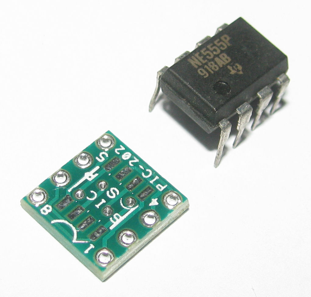
  • A component with polarity +/- should have silkscreen indicating the component’s polarity. (Diode, LED, IC, Capacitor, etc…)
  • If space permit, print the component value next to the component.
  • Design surface mount component. It saves space and is easier to assemble compared to through hole components.

Quick PCB Design Checklist before sending for PCB fabrication

Here is a quick checklist to go through after you design the PCB board. This check list wraps up the additional details completing your PCB board design.

  • Mounting hole for PCB board. (usually 3.2mm hole for M3 screw size)
  • Ensure the input and output port connector is properly labelled for the user.
    for example:

    • Pwr In, + 12V –
    • LED indicator, RUN, COMM, ERROR
    • Switch and Jumper pins.
    • Input-Output Connector, Port01, Port02, +/-
    • Ethernet, RS232, RS485
  • Label for the name, product code and version for the PCB design.
    for example:
    USB I/O Controller
    PIC-304 ver1.0
    Made In Singapore
  • Labelling of components and its value on the PCB board to aid in the production.
  • Setup some test pin or pad for production testing process, verifying for the valid voltage.
    • check for power input voltage
    • check for regulated voltage
    • check for analogue circuit voltages

Typical PCB material specification

Before any PCB fabrication is started, you will need to specify the type of material to be used for your PCB. There are many types of material specification. For a typical industrial grade PCB material, it is recommended to use the commonly available,
Typical PCB specification: FR4, 1.6mm, 2L, 1oz copper, Green Mask, White Silk, HASL.

  • FR4 is the fiberglass material PCB board. There are also other type of PCB board materials. Some cheaper cost, lower durability. Some are used for specific high frequency application, which can be more expensive. FR4 is the most commonly available material and good enough for most application.
  • 1.6mm is a common PCB thickness. Most components, connectors (RJ45, DB9) footprint uses this standard thickness.
  • 2L means 2 layer PCB board.
  • 1oz copper is the thickness of the copper layer. 1oz is good enough for most application. If your trace is small and current flowing through is high, you may like to increase it to 2oz or more to minimise the heat that can be generated from the trace.
  • Green Mask, the color of the mask which is also the PCB board color. Some of the commonly used color are blue, red, black, white, etc… Green mask is still the best, trace is more visible.
  • White Silk, specify the color of the silkscreen printing use for all the components and connectors labeling.
  • HASL (Hot Air Solder Leveling) specify the type of plating/costing to the exposed copper pad. Without the coating, it means that the expose surface will be bare copper. Leaving the copper surface expose to the air can result in oxidation on the surface. Once the pad is oxidation, soldering will become difficult. Even if it can be soldered, the soldered joint will not be good. This may cause intermediate issue when your circuit board is operating. There are many type of finishing. Gold plating is one of the options. A minimum plating thickness is required to minimise oxidation. Gold is expensive and is typically not needed. HASL is simply a coating of solder on the copper pad to prevent it from oxidation. It is a common cost effective method.

You can also check out more details of this recommended PCB specification on this page.

These are the basic things you should take note when designing your own electronic PCB circuit. If you need further assistance regarding PCB design or electronic circuit design, feel free to contact PIC-CONTROL using the message form on the right side bar of this page.

Wireless Tracking System

Wireless Tracking Technologies

A wireless tracking system can help to track the number of objects at the different zone. There are many tracking solutions on the market now that offers object tracking for indoor application. These are some of the tracking technologies available today.

  • iBeacon
  • BLE (Low Energy Bluetooth)
  • Active RFID Tags
  • UWB beacon (Ultra Wide Band Width)
  • Zigbee
  • Wifi

Tracking of objects or devices can help automate or improve the efficiency of a business process. The location information captured can also be analysed to provide with further insight to further grow and expand your business.

While there are many benefits to deploying a tracking system for your business operation, there are disadvantages in using these tracking technologies for tracking of a large number of tags.

Disadvantage of the Current Tracking Technologies

The listed tracking technologies are quite advanced in the implementation. They use protocol communication to uniquely identify tags or beacons. For an application that requires a larger quantity of tags (tracking carts or trolleys), these advanced tracking technologies will not be suitable.

Unable to Handle a Larger Quantity of Tags

Expensive Tags

Each tag has a receiver and transmission to communicate with each other. On board the circuit, a microcontroller or data logic is required to process the data from the communication. More components and IC chip is required in order to build a beacon tag.

These technologies might be useful or low quantity tracking of unique objects. For tracking of a large quantity of trolley or carts, these tags are perceived to be more expensive for the value they are adding to the application.

Higher Energy Consumption

More components used can mean a higher energy consumption. The complex communication protocol makes the tag work even more. Given the often limited size of the wireless tag, the tag’s battery would probably drain flat faster.

Slower Response Time

The complex protocol and a large number of tags competing for the communication air time are going to cause more data collision, re-transmission and hence slower response time.

Alternative Tracking Solution (Wireless RF Beacon)

A simple RF beacon is proposed to help track massive mobile objects can be design and implemented.

The beacon uses simple RF pulse to alert the base station. It is a low-cost solution for tracking of a larger quantity of mobile objects like trolleys and carts.

Advantages

  • Lower cost of tags.
  • Lower energy consumption of tags, longer operating time.
  • Handle a larger quantity of tags.
  • Provide an estimated quantity of tags within a zone.
  • Ability to deploy multiple base station to improve the resolution of the tag tracking.
  • Simple technologies, simple to maintain.

Disadvantages

  • Unable to uniquely identify the object (cart, trolley).
  • Unable to precisely count the number of objects.
  • The tags are unable to exchange data with the base station.

Simple Tracking Solution For Massive Mobile Objects

While there are many advanced technologies to perform object localisation, tracking and monitoring, it may not be the best solution for application that does not need the objects to be uniquely identified.

A cost effective wireless RF beacon is proposed to help cater the application of counting the number of objects within a given zone to enhance the productivity and business operation.

Freelance Electronic Engineer

Are you looking for a freelance electronic engineer to help you with your electronic engineering project, design or electronic hardware product troubleshooting? You can check out the following resources for a freelance electronic engineer in Singapore, and overseas.

If you are ready to outsource your electronic project, consider engaging a specialised electronic engineering company to managed your electronic design project. For more information about our electronic engineering services, check out our website or contact us directly.

Freelance Electronic Engineer (Jobs in Singapore)

Singapore has one of the largest electronic engineer graduates from the South East Asia region. There is a large pool of engineers graduated from our local university, polytechnic and ITE each and every year. Electronic graduates represent about 20% of the total graduates in Singapore. There is no shortage of engineering professional in Singapore.

For a business operating in Singapore, it will be easier to engage with a local freelance electronic engineer. Engineering can be complex at times and communication is very important in getting across what you are looking for.

A local freelance engineer shares a common language and culture. It is easier to communicate and easier for them to understand the nature of your projects. There will be times where a meetup and discussion is necessary. A local freelance electronic engineer can provide much more flexibility and security.

The following are some of the links where you can engage electronic engineer freelancer in Singapore,

Typical hiring rate for electronic professional is about $500/day (year 2011) in Singapore. Compare to hiring permanent engineering staff, there is a much lesser the responsibility and burden for your business operating cost.

Freelance Electronic Engineer (Overseas)

Engaging an overseas freelancer engineer takes more effect. It is important to select one who is able to communicate very well with you. Very often you will want them to be responsive.

There is a lesser chance of meeting up face to face with your freelancer. It is always better to engage with an online platform to help you manage the project transaction like the deliveries and payment issue. An online platform also provides scoring and review system which can help you determine the service that you are getting from the freelancers base on their completed project in the past.

The following are some of the links where you can engage electronic engineer freelancer from overseas,

Hire your electronic engineer from

The risk is often higher engaging engineers from overseas unless the project is very simple. However, there is a greater potential to discover more good engineers from a wider pool of resources overseas.

Alternative to Freelance Electronic Engineering Solution

PIC-CONTROL is an electronic engineering service company providing design and product manufacturing services to our client. We work closely with you to helped realised the solution for your business needs.

Advantages of outsourcing to a specialised electronic engineering company,

  • Comprehensive resources and an established network to solve your problem.
  • Rich experience, highly specialisation and interest in the electronic industry.
  • Guarantee delivery.
  • Maintaining documentation for your projects.
  • Warranty and technical support.
  • Always available for you.

PIC-CONTROL has the expertise, resources and network in the area of electronic engineering to bring your business forward. We are your engineers taking care of your engineering projects.

Check out our website for further information, or contact our sales engineer today.

Hammond Enclosure

List of low profile electronic enclosures from Hammond Manufacturing that are less than 30mm in height.

Visit Hammond Manufacturing website for more other electronic enclosure products.

Hammond Product Code Length (mm) Width (mm) Height (mm) Appro. Circuit Width Space

Aluminum Extrusion Enclosure Box 1455

1455 (Metal End)

1455 (Plastic End)

  • 80
  • 100
  • 120
 70 12 ## x 57.3 x 4.45mm
  • 80
  • 100
  • 120
 71.7  19   ## x 57.5 x 11mm
 *
  • 80
  • 120
 54 23   ## x 48 x 16mm
 *
  • 60
  • 80
45 23  ## x 35.6 x 16mm
 * 120 78 27   ## x 70 x 16mm
*

80

103 31
Other Variation

 Models with open-able top panel.

https://www.hammfg.com/1455V2.htm

  • 1455J1202
  • 1455K1202
  • 1455L1202
  • 1455N1202
  • 1455J1602
  • 1455K1602
  • 1455L1602
  • 1455N1602
  • 1455P1602
  • 1455Q1602
  • 1455R1602
  • 1455T1602
  • 1455L2202
  • 1455N2202
  • 1455P2202
  • 1455Q2202
  • 1455R2202
  • 1455T2202
Click links above for spare part and accessories.

 Screw for project:

Button Head Socket Cap Screw
6-32 x 3/8″ (length) x 0.375″ (pitch)

Aluminum Extrusion Enclosure Box 1457

  • 120
  • 160
84 28.5
  • 80
  • 120
59 30.9
  • 120
  • 160
104 32
Click links above for spare part and accessories. Option for
Mounting Flange

1551

(*Face Panel)

Max PCB Size
1551N 35 35 15 29.5 x 29.5 x ??mm
1551M 35 35 20
1551Q 40 40 15 34.5 x 34.5 x ??mm
1551P 40 40 20
1551F 50 35 15 44 x 29 x ??mm
1551G 50 35 20
1551S 50 50 15
1551R 50 50 20
1551J 60 35 15 54.5 x 29.5 x ??mm
1551H 60 35 20
1551L 80 40 15 74 x 34 x ??mm
1551K 80 40 20

1591

1591XX “TBU” Translucent ABS

1591XX “S” Economical

1591XX FL Flame Retardant with Flanged

1591XX “S” FL Economical with Flanged

1591XX “T” Translucent Polycarbonate

1591R RFI Shielded

1591XXA 100 51 22 94 x 44.5 x ??mm
1591XXM 85 56 24 80.7 x 51.51 x ??mm
1591XXB 113 63 28 108 x 57.5 x ??mm

1593

1593 Translucent

(*End Panel)

No. of Panels Battery Compartment
1593D 114 36 25 2 0
1593S 92 66 21 1 1
1593T 112 66 21 1 1
 * 1593K 66 66 28 2 0
1593J 66 66 28 0 0
 * 1593L 92 66 28 2 0
1593P 92 66 28 1 1
1593Q 112 66 28 1 1
1593X 140 66 28 2 0
1593Y 140 66 28 1 1
1593N 110 75 25 2 0
1593BB 95 77 30 2 0

1594

1594 “W” Water Tight

1594 “S” Economical

1594 RFI Shielded

1594 RFI Shielded (conductive plastic)

(*Face Panel)

1594A 56 56 28
1594B 81 56 28
1594C 105 66 33

1599B

1599 RFI Shielded (conductive plastic)

(*Face Panel)

Belt Clip Battery Compartment
* 1599BBK 130 65 25 0 0
1599BBKBAT 130 65 25 0 1
1599BBKCP 130 65 25 1 0
RITEC (Hand Held) Battery Compartment
RH3115 100 60 25 0
RH3115A 100 60 25 1
RH3135 120 70 25 0
RITEC (Hand Held with Battery Door)
RH3011BK 130 68 25
RITEC (short length, long width for instrumental)
RM Series
130 100 30
130 100 50
130 100 70
190 140 30
190 140 50
190 140 70
250 180 50
250 180 75
250 180 100

TSSOP to DIP Adapter (2.54mm)

Convert your TSSOP SMD IC chip to DIP using an SMD adapter board for your electronic design rapid prototyping.

TSSOP (0.64mm) to DIP Adapter (2.54mm)

TSSOP 8 pins 0.64mm pitch to DIP 2.54mm pitchfor TSSOP pitch 0.64mm (pins spacing).

Suitable for TSSOP package up to 8 pins.

Click here to buy PIC-202 SMD Adapter Board.

or visit our product page for further details about PIC-202 SMD Adapter Board.

TSSOP (0.635mm) to DIP Adapter (2.54mm)

SMD IC adapter, SMD to 2.54mm pitch [PIC-201]for TSSOP pitch 0.635mm (pins spacing).

Suitable for TSSOP package -> 16 pins, 18 pins, 20 pins, 24 pins, up to 28 pins.

Click here to buy PIC-201 SMD Adapter Board.

or visit our product page for further details about PIC-201 SMD Adapter Board.

More Electronic Prototyping Solution

Check out our other rapid prototyping board products.

PIC-CONTROL also provides rapid prototyping services for electronic product development.

uMAX to DIP Adapter (2.54mm)

Convert your uMAX SMD IC chip to DIP using an SMD adapter board for your electronic design rapid prototyping.

uMAX (0.5mm) to DIP Adapter (2.54mm)

SMD IC adapter, SMD to 2.54mm pitch [PIC-201]for uMax pitch 0.5mm (pins spacing).

Suitable for the uMAX package up to 10 pins.

Click here to buy PIC-201 SMD Adapter Board.

or visit our product page for further details about PIC-201 SMD Adapter Board.

uMAX (0.65mm) to DIP Adapter (2.54mm)

SMD IC adapter, SMD to 2.54mm pitch [PIC-201]for uMax pitch 0.65mm (pins spacing).

Suitable for the uMAX package up to 8 pins.

Click here to buy PIC-201 SMD Adapter Board.

or visit our product page for further details about PIC-201 SMD Adapter Board.

More Electronic Prototyping Solution

Check out our other rapid prototyping board products.

PIC-CONTROL also provides rapid prototyping services for electronic product development.

SSOP to DIP Adapter (2.54mm)

Convert your SSOP SMD IC chip to DIP using an SMD adapter board for your electronic design rapid prototyping.

SSOP (0.635mm) to DIP Adapter (2.54mm)

SMD IC adapter, SMD to 2.54mm pitch [PIC-201]Suitable for SSOP package -> 16 pins, 18 pins, 20 pins, 24 pins, up to 28 pins.

for SSOP pitch 0.635mm (pins spacing)

Click here to buy PIC-201 SMD Adapter Board.

or visit our product page for further details about PIC-201 SMD Adapter Board.

SSOP (0.64mm) to DIP Adapter (2.54mm)

TSSOP 8 pins 0.64mm pitch to DIP 2.54mm pitchfor SSOP pitch 0.64mm (pins spacing).

Suitable for SSOP package up to 8 pins.

Click here to buy PIC-202 SMD Adapter Board.

or visit our product page for further details about PIC-202 SMD Adapter Board.

More Electronic Prototyping Solution

Check out our other rapid prototyping board products.

PIC-CONTROL also provides rapid prototyping services for electronic product development.

QSOP to DIP Adapter (2.54mm)

Convert your QSOP SMD IC chip to DIP using a SMD adapter board for your electronic design rapid prototyping.

QSOP (0.635mm) to DIP Adapter (2.54mm)

SMD IC adapter, SMD to 2.54mm pitch [PIC-201]Suitable for QSOP package -> 16 pins, 18 pins, 20 pins, 24 pins, up to 28 pins.

for QSOP pitch 0.635mm (pins spacing)

Click here to buy PIC-201 SMD Adapter Board.

or visit our product page for further details about PIC-201 SMD Adapter Board.

QSOP (0.64mm) to DIP Adapter (2.54mm)

TSSOP 8 pins 0.64mm pitch to DIP 2.54mm pitchfor QSOP pitch 0.64mm (pins spacing).

Suitable for QSOP package up to 8 pins.

Click here to buy PIC-202 SMD Adapter Board.

or visit our product page for further details about PIC-202 SMD Adapter Board.

More Electronic Prototyping Solution

Check out our other rapid prototyping board products.

PIC-CONTROL also provides rapid prototyping services for electronic product development.

SOT23 to DIP Adapter (2.54mm)

Convert your SOT23 SMD IC chip to DIP using an SMD adapter board for your electronic design rapid prototyping.

SOT23 to DIP Adapter (2.54mm)

SMD IC adapter, SMD to 2.54mm pitch [PIC-200]Suitable for SOT23 package -> 3 pins (SOT23-3), 5 pins (SOT23-5), 6 pins (SOT23-6), up to 12 pins.

Click here to buy PIC-200 SMD Adapter Board.

or visit our product page for further details about PIC-200 SMD Adapter Board.

More Electronic Prototyping Solution

Check out our other rapid prototyping board products.

PIC-CONTROL also provides rapid prototyping services for electronic product development.

SOIC to DIP Adapter (2.54mm)

Convert your SOIC SMD IC chip to DIP using a SMD adapter board for your electronic design rapid prototyping.

SOIC (1.28mm) to DIP Adapter (2.54mm)

SMD IC adapter, SMD to 2.54mm pitch [PIC-200]for SOIC pins package -> 16 pins, 18 pins, 20 pins, 24 pins, up to 28 pins.

Suitable for narrow or wide SOIC IC chip body.

Click here to buy PIC-200 SMD Adapter Board.

or visit our product page for further details about PIC-200 SMD Adapter Board.

SOIC-8 (1.28mm) to DIP Adapter (2.54mm)

soic08 to dip08 adaptorfor SOIC pitch 1.28mm (pins spacing).

Suitable for SOIC 8 pins package.

Click here to buy PIC-202 SMD Adapter Board.

or visit our product page for further details about PIC-202 SMD Adapter Board.

More Electronic Prototyping Solution

Check out our other rapid prototyping board products.

PIC-CONTROL also provides rapid prototyping services for electronic product development.