|
When
I first got to learn about this power saver product during an
exhibition in Singapore, I was a little bit surprise about it. The
meter measuring
the current drop instantly when this power saver thing was turned on.
The surprising part is not about its energy saving performance, but the
fact that business people is really smart. How they are able to make
use of a electrical physics to convince consumer into buying the
product.
Myself, I am trained in Electrical & Electronics Engineer for my
diploma and degree course. Although I have graduated from my university
many years back, I had little experience in the field of the 230Vac
single phase voltage system that we are using in our home. Nevertheless
I am able to recognize what I was being presented in the exhibition.
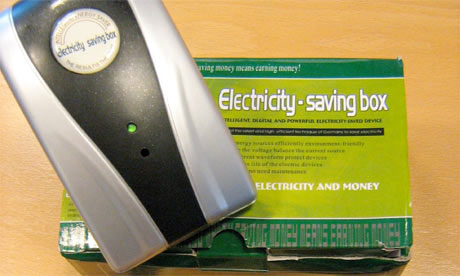
The power saver device is a scam. The purpose of dedicating this
webpage is for me to present to those who have doubt in the device, to
understand more about the power saver in a simple and experimental way.
To let you see clearer how the scam works, and how you can see the
fraud even at the exhibitor’s own setup.
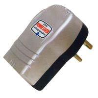
Two things in common when power saver is presented to the consumer. You
will always be presented with an instrument call ammeter (or current
meter). The appliance used in the demonstration are of inductive
property (eg. motor, fan, ballast lamp). These are the two main
ingredients that will make the presentation looks convincing for a
non-electrical trained consumer.
The ammeter was there to show the reading of the electrical current
flowing through the power cable which is connected from the mains to
the operating appliance. Higher current reading will means that more
electrical current is being drawn from the electricity power grid.
There are no tricks on this measurement, they are real. That was why
everytime when the power saver is turned on, you were able to see the
immediate drop in the electrical current. Most of the demonstration
using a clamp ammeter. The meter is clamp to either the electrical live
or neutral cable and is able to measure the magnetic field around the
cable. The intensity of the magnetic field is proportional to the
current flowing through the cable, that is why the current can be
measured. The clamp meter is easy to setup and customer can easy be
convince since the setup is clean not not hidden from the consumer’s
sight.
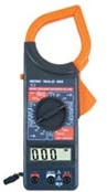 A
picture if the clamp-ammeter for measuring the current flowing through
your electrical appliances. Clamp the live or neutral wire of your
electrical cable to measure the current flowing. A
picture if the clamp-ammeter for measuring the current flowing through
your electrical appliances. Clamp the live or neutral wire of your
electrical cable to measure the current flowing.
The problem lies in the engineering knowledge which consumer is not
aware about. Having the current reduced does not mean that the power
consumption will be reduced. Most people will tends to link the idea of
a reduce in current, to a reduce in energy consumption. This concept
seems a bit illogical, but this is the real situation. Current and
power are not directly related. Real energy consumption is determine by
the wattage consumption, and not the current.
The actual technical terms are call real and imaginary power. They can
be quite difficult to understand and I shall simplify it by not going
too deep into the actual technical details.
There are 3 types of load/appliances that the electrical grid will
deliver its power to. They are resistive, inductive and capacitive
load. Inductive and capacitive are technically not efficient because
extra current has to be drawn from the electrical grid in order to
support the appliances. We call these load reactive load. Assuming a
household appliance that consume 100W of power. No matter what type of
load (resistive, inductive or capacitive) this appliance might be, the
real power consumption of this appliance will be 100W. This means that
the energy consumption should remains the same regardless of the load.
Most appliances that we have at home are of resistive and inductive
nature.
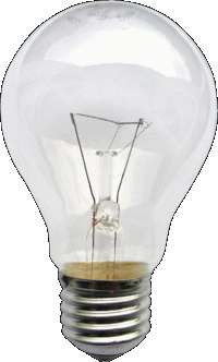
Appliances at home that are Resistive in nature are,
– hot iron
– heater
– oven
– incandescent bulb
Appliances at home that are Inductive in nature are,
– fan
– fridge
– air-con compressor
– washing machine
– vacuum cleaner
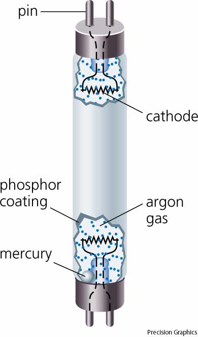
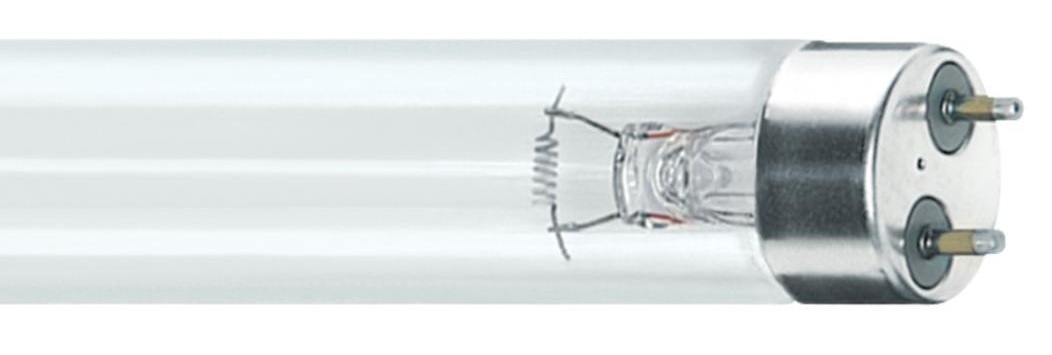
– magnetic ballast fluorescent lighting
The only thing different between the type of load, is the current being
drawn. For example this appliance is a 100W resistive load, drawing a
current of 0.4A from the grid. This 0.4A will be the lowest current
that a 100W load can go.
Example 1:
Power Supply —————————————–> 100W
Resistive Appliances
Flowing Current 0.4A
If the 100W load is now inductive or capacitive in nature, we will
expect a current reading more than 0.4A. This is because such a load
requires more current to support the load. Inductive and capacitive
load is a form of energy storage component for the electricity. The
100W inductive load though draw in more current from the power grid to
fill its storage tank, it will not consume all the energy. The unused
current will flow back to the grid. This extra in/out flow of the
current is the reason for the rise in the current that we will measured.
Example 2:
Power Supply —————————————–> 100W
Inductive Appliances
Flowing Current 0.6A
How much this extra current will be, will depend on the power factor.
Power factor ranges from 0-1. It is an indication of the load type. A
power factor of maximum 1.0 indicates a pure resistive load will have a
minimum current. A power factor of 0.0 indicates a pure capacitive or
inductive load will encounter the maximum current. Any power factor
reading between 0.0 to 1.0 means that the load is a combination of
both.
This power factor thing can be corrected like a see-saw as illustrated
below..
Power factor 0.0————————–1.0
————————–0.0
…………inductive————————resistive————————capacitive
Example 1 is a resistive load 100W 0.4A. The power factor will
definitely be 1.0 .
Example 2 is an inductive load 100W 0.6A. The power factor could be
let’s say 0.5.
The load being too much inductive with a power factor 0.5A can be
corrected by installing a capacitive counter load in parallel. The
correct capacitive load can pull up the power factor to 1.0. Too little
capacitive counter load will not pull the load fully to the balanced
power factor of 1.0. On the other hand, too much of the capacitive
counter load will make the overall load capacitive in nature and hence
power factor will also be lower than 1.0. The key to attain a power
factor of 1.0 is by using the correct counter blance load. Attain a
power factor of 1.0 will reduce the current to its minimum.
The power saver is actually a pure capacitance component inside with
its value unknown. The demonstration appliance is typically a motor or
magnetic ballast fluorescent lamp which is inductive in nature. When
the inductive appliance is turned on, the current measured will consist
of the extra current flow, therefore reading is higher. When the power
saver is turned on at the same time, the load is though balanced with a
power factor nearer to 1.0, therefore current is now lower. The closer
the counter balance is matched, the low the current will be. The lowest
current it can go will be based on its wattage as if it is a resistive
load. But it is not easy to match it to exact power factor of 1.0 for a
typical consumer.
As
what I have understood, the power service provider do not charge
consumer on the current that we have drawn, but on the real power that
we have used up. It will not be fair if they charge us base on the
current, because although we might draw higher current, we also
returned the unused portion back to the grid.
For
factory and industrial, the situation is slightly different. They will
be charged on the extra current for the reactive load that they have
introduce. Why is there such a different? This is because the
industrial ususally draw very high current from the grid. If the
current is high, the cable to support the high current has to be
thicker. If the industrial user do not correct the factor of their
manufacturing plant, it will be at the expense of the service provider
to lay more cables for them. For industrial user, they will be charged
base on the real power and the reactive power that they use. For home
consumer, our usage is quite predictable and insignificant.
So
unless your power meter measure and charges you on both the real and
reactive power, you will not need to correct the power factor for your
own house.
High current uses thicker cable. Cable not
thick enough, heat will be generated. This is a form of cable loss.
This is also how a safety fuse for electrical system works. The fuse
will burn itself if the current is too high.
But
wouldn’t that means that the cable out from the power station will be
very very thick to support the whole population? Yes, but there is
another solution. The voltage from the power station is very very high.
Given a limited cable size, we can still deliver more power to the
population by increasing the voltage. Power is the product of voltage
and current. With the limit in cable size, hence the current, we can
deliver more power by rising the voltage. That is why you can often see
electrical sub-station around the place we live in. It is a big
transformer inside which step down the very high voltage to a lower
voltage that we can use. There are many stages of sub-station from a
power station all the way to the end consumer.
You
can think of the electrical system as the distribution for our water
pipes. High voltage is similar to high pressure for the water pipe.
Cable size or current is the water pipe size. Electrical power being
the volume of the water. Having a limitation in the waterpipe size does
not means that we cannot deliver more water to the population. We can
still increase the water pressure so that the water is able to travel
faster, hence deliver more water though the pipe out.
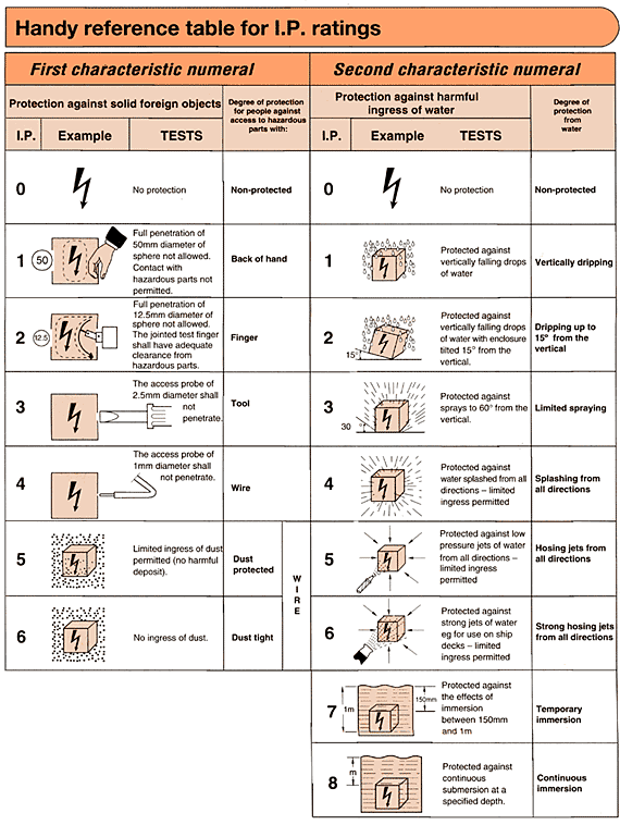
The Experiment
Now that we have know something about power factor correction, the
following experiment setup will further illustrate the function of a
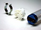
power saver and how the thing works. I have done some reverse
engineering work on the following 3 items shown in the picture consist
of (from the left)
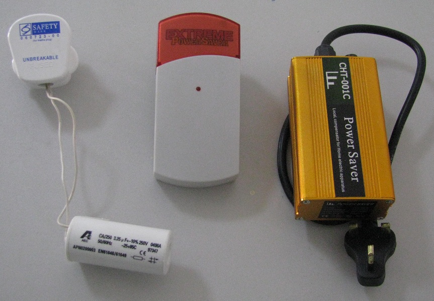
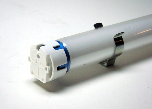
1)
I have managed to salvage white cylindrical AC capacitor from an office
fluorescent lighting using a magnetic ballast. I had remembered seeing
such component connected to the setup and have dismantled one for the
experiment. It is just an ordinary AC capacitor which electrical
contractor sometimes used to correct the power factor of the lighting
so that current flowing from the mains supply to the lamp can be
minimum. The magnetic ballast is an inductive component. Having this
counter balance capacitor load, the power factor can be improve,
therefore reduce the current. This capacitor was connected to a 3 pin
plug for the experiment. Using a multimeter, I managed to measure the
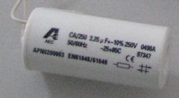
capacitance to be 3.2uF, which is the same value as labelled on the
component itself.
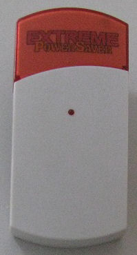
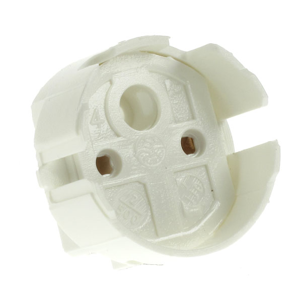
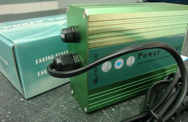
2)
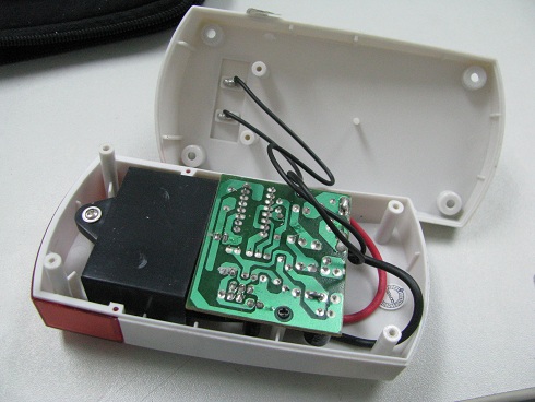
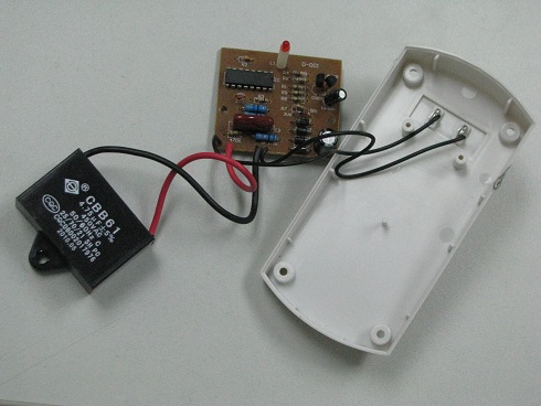
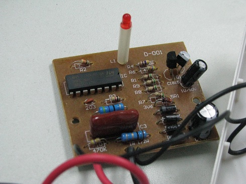
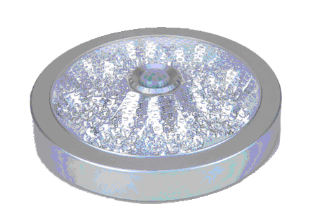
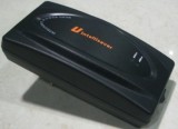
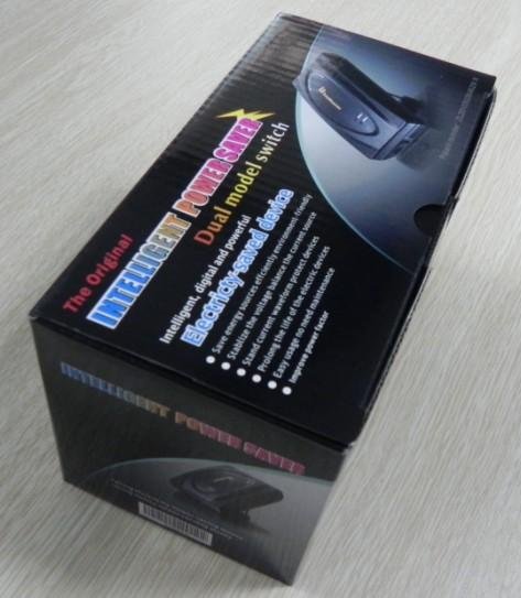
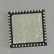
GAD1203 Extreme Power Saver (CX005). I have managed to open it up to
understand further about it’s interior. The inside consist of a circuit
and a black rectangular block. At a glance, it seems quite complicated
circuit, but after careful examination, the circuit looks suspicious.
The IC chip on-board is a logic gate IC which does not do any function.
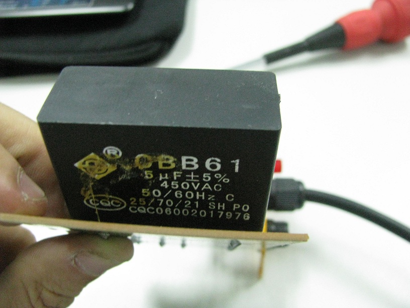
The black box is actually a 4.75uF capacitor component. The measured
capacitance is 5.6uF which is quite close to the label. The incoming 2
pin Live and Neutral is connected parallel to the capacitor and the
circuit. Without the circuit, the capacitor will be enough to act as a
power factor correcting device.
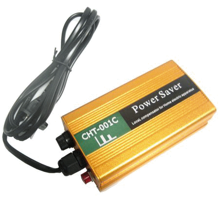
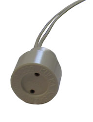
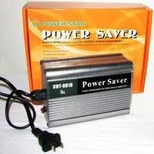
3)
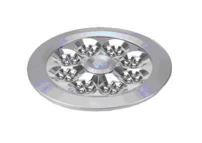
GAD1202 Power Saver (CHT-001C), 2400W. This product is easier to do the
reverse engineering. It consist of two black box connected in parallel
to the AC Live & Neutral wire. The 2 black box is the capacitor
measuring 5uF each which is the same as labelled on the component
itself. Two capacitor means that the total capacitance is 10uF. There
is a lamp indicator which is connected to the AC line, indicating that
the device is connected to the AC mains.
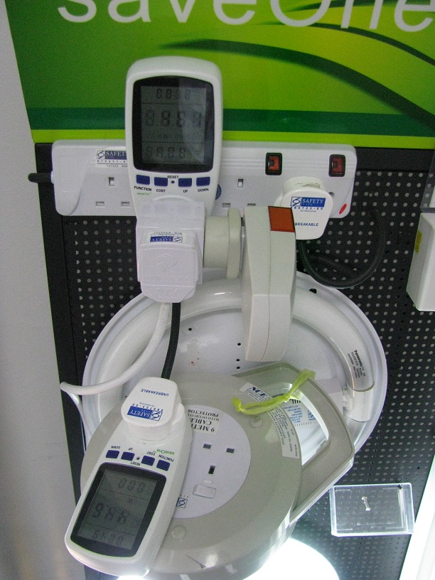
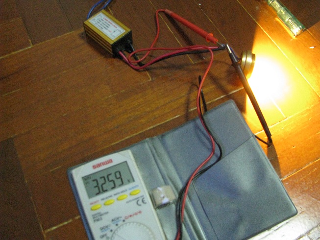
I have this experiment and
setup as below with help from saveOne Pte
Ltd
in Singapore. Their business is mainly in the Asia region Philippines,
Thailand, Malaysia and China. This company sells a range of energy
saving products, from energy saving lighting, energy saving electronic
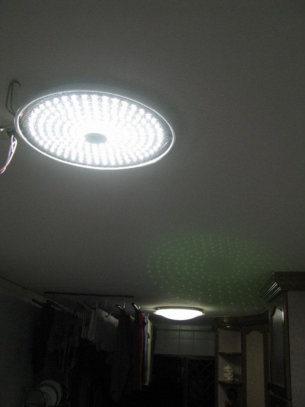
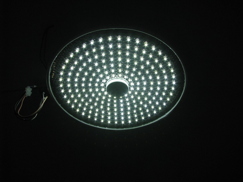
ballast to energy saving equipments. The picture shows a demonstration
rack of their electronic
ballast
product for circular fluorescent lamp which I have also installed for
my house. I like the product and have written an article about it quite
some time ago. If you are interested, you can visit this link.
The
reason I use this rack for the experiment because there was this
magnetic ballast fluorescent lamp setup at the bottom of their rack.
You can see from the picture, it is the lamp that is lighted up.
Magnetic ballast component is an inductive load and is useful for our
experiment.
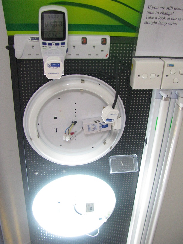
The
setup consist of 2x power meter to check on the wattage, current and
power factor at 2 location along the power supply line from the mains
to the magnetic ballast lamp. Right from the top, you can see a 4 way
socket power extension. This is the point where I would tap the power
from. The first thing that was connected is the power meter
which was connected to the 2nd socket position. This power meter no.1
measures the electricity for the whole setup. The later setup that
would be connected to this power meter will be measured. This means
that we would be able to know the current flowing from the supply mains
to this setup, and also the wattage consumption of the setup.
From
the power meter no.1, a multi-plug socket was plugged on top of it to
split the power outlet into 2. On the right side, it is where the power
saver (capacitor under test) will be plugged. The front side is the
3pin plug which is from the cable extension drum. On top of the cable
drum is power meter no.2. The magnetic ballast lamp is connected to
this power meter no.2. Power meter no.2 measures the wattage, current
and power factor for the lamp.
Measure Result from Power Meter no.1
| S/N |
Power Saver or
Capacitor connected |
Watt |
Current |
PF |
| 0 |
Without any capacitor connected
|
44.2W |
0.432A |
0.42 |
| 1 |
Capacitor 3.25uF ±10% 250V
|
44.2W |
0.242A |
0.76 |
| 2 |
GAD1203 Extreme Power Saver (CX005), 5.6uF
|
45.1W |
0.198A |
1.0 |
| 3 |
GAD1202 Power Saver (CHT-001C), 10uF
|
45.3W |
0.403A |
0.47 |
0.
Without any thing connected, the magnetic ballast lamp consume a
wattage of 44.2W. Current is high at 0.432A. The power factor measured
from the power meter
is low at 0.42.
1.
When the small 3.25uF capacitor is connected along the power line, the
measurement from power meter no.1 shows that the power factor has
improved to 0.76. The improve in power factor will also lead to a drop
in the current. With this small capacitor, the current is now lower at
0.242A. The power consumption remains unchanged for the own setup.
2.
Next comes the Extreme Power Saver GAD1203. The 5.6uF capacitance is
higher than the previous 3.25uF. As shown in the measurement, the power
factor is now exactly 1.0. This is a perfect match. The magnetic
ballast requires 5.6uF capacitance to correct its power factor. The
current is measured to be 0.198A. Since the power factor is perfect,
this is the lowest current we can attain for the lamp. The power
consumption goes slightly higher at 45.1W, probably due to the extra
circuit that is in the Power Saver.
3. Next comes the
GAD1202 Power Saver. The 10uF capacitance is among the highest of all
the Power Saver under this test. When it is connected along the line,
the power factor actually drop down to 0.47. This happens because we
have over correct the power factor by putting in too high a capacitance
value. The drop in power factor comes with an increase in the current
flow of 0.403A. Putting too much Power Saver can degrade the
performance. It is possible to create an even higher current than the
original setup (without any thing connected along the line). This means
that if too many Power Saver is connected along the line, you will
expect an increase in current instead. You can try it out on the
demonstration, requesting the salesman to install more Power Saver to
the setup. The current will drop up to a certain point then increase
more and more after that. The current will never drop back once the
power factor is over corrected. You will need more inductive load to
balance it back to a power factor of 1.0. I have tried it out before,
and was able to see the increase in current once the second Power Saver
was plugged in. The wattage is the highest among the rest at 45.3W.
This might be due to the lamp indicator in the circuit which will also
consume energy.
Measure Result from Power Meter no.2
Throughout
the turning on and off of the Power Saver device, the reading remains
the same. The reading is the same as the Power Meter no.1 as if no
capacitor or power saver is connected. This shows that current from the
Power Saver all the way to the inductive load (magnetic ballast
fluorescent lamp) was not corrected and still remains high at 0.432A
throughout the experiment.
Conclusion
The
current was corrected only from the power supply mains to the Power
Saver only. Current from the Power Saver to the inductive load remains
the same. In order to keep the current minimum along the cable, the
power saver will be better kept as close as possible to the load that
requires power factor correction.
The use of a power
factor correcting device helps to reduce current from the power mains
to the device. Lower current means that the current carrying AC cable
can be afford to be thinner. To put it in another way, more inductive
appliances can be connected to the same AC cable if they are all power
factor corrected. Lower current flowing through the cable also means
less power loss on the cable it self. High current flowing through a
thin cable can generate some heat (cable loss). However cable loss is
usually insignificant.
To conclude, the power saver can
help to reduce current flow. In order to reduce the current, you will
need to understand your load and apply the correct counter load value.
Over correcting an appliances will make it worst. In terms of energy
saving, the saving will be insignificant. In fact, the experiment shows
a slight increase in wattage. It is quite conclusive that the Power
Saver product is a scam.
The following are some other sites from people who have
similar knowledge and explaination. I have collected these website
for your further understanding of how power saver works.
http://www.nlcpr.com/Deceptions1.php
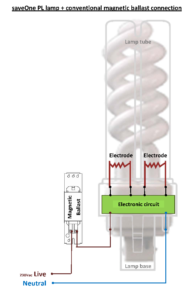
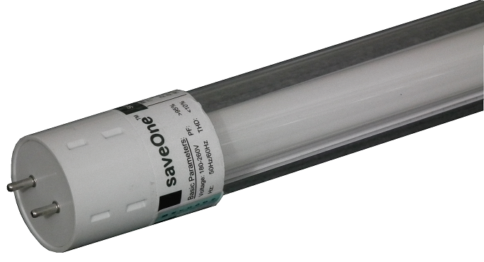
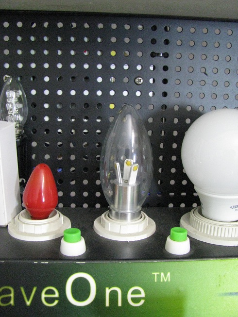
For alternative power saving method, you may also like to find out
about voltage trimmer from saveOne, which offers power saving
solutions. Some of their products are listed below for reference.
|


 and a fluorescent tube
  to work.
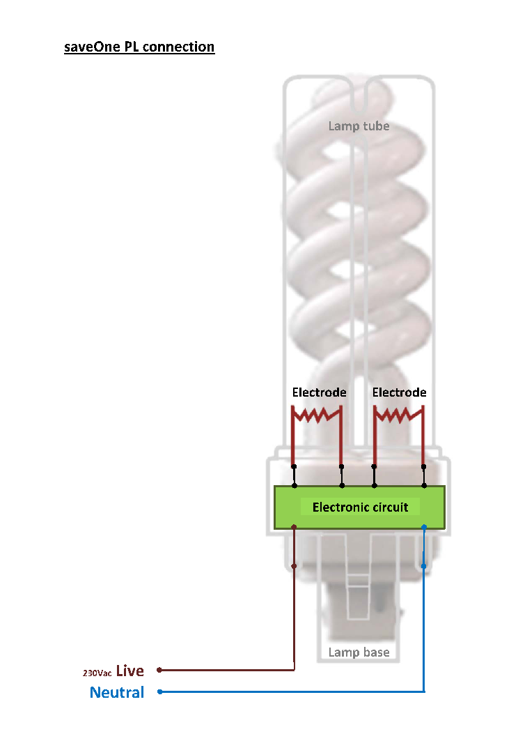


 Front
Front Back
Back


 RC filter, the simplest low pass filter.
 Another way of looking at the same RC filter.
  A capacitor as a low pass filter.
 RC filter, the simplest high pass filter.


 A
phone small enough to carry around.
A
phone small enough to carry around.


 Mobile
phone as thin as biscuit.
Mobile
phone as thin as biscuit.


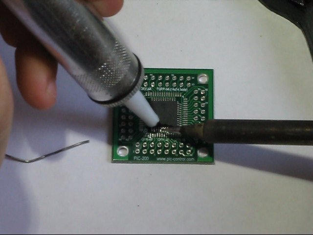
 Rework Station


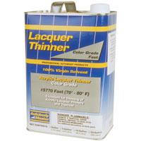

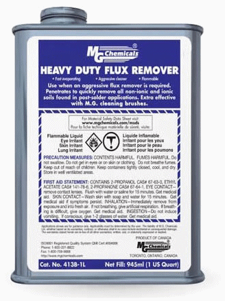


 Alcohol
& thinner has a lower flash point, and catch fire easily. You have to be
extremely in handling and storing these flammable chemical. Do not store or
work on the chemical near electrical appliances, hot area or things that can
cause spark. Keep your windows open to allow air to circulate while working
with these chemical. They may cause headache, dizziness and uncomfortable
when inhaled.
Alcohol
& thinner has a lower flash point, and catch fire easily. You have to be
extremely in handling and storing these flammable chemical. Do not store or
work on the chemical near electrical appliances, hot area or things that can
cause spark. Keep your windows open to allow air to circulate while working
with these chemical. They may cause headache, dizziness and uncomfortable
when inhaled.


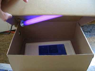

 ultra-violet exposure


 When mixing
NaOH to water, heat will be produce. Stir the water solution constantly
while adding in NaOH slowly.
When mixing
NaOH to water, heat will be produce. Stir the water solution constantly
while adding in NaOH slowly.


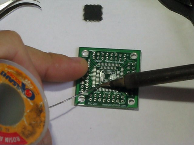
 tinned PCB board.


