Introducing PIC Microcontroller projects
Written by Lim Siong Boon, last dated 20-Oct-09.
|
PIC Microcontroller
|
|
References: Microchip dsPic 30F Programming reference guide
|


Singapore Customized, custom made Electronics Circuits & Kits
|
Development Tools History
|
|||||||||||||||||||
|
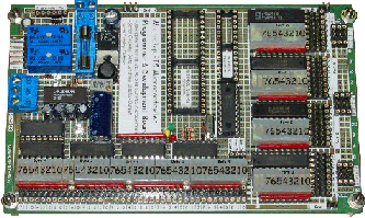
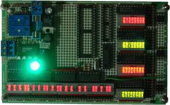
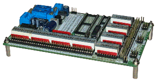
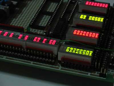
PIC microcontroller Development Board (Completed on 2006-10-28) The ultimate PIC Microcontroller development board. After years of programming PIC microcontroller, I have finally design my super development board to program PIC microcontroller firmware. The automatic programming mode select and the 40 bits LED light bar display have ease my programming process and increase debugging speed by 10 times. I can easily do troubleshooting because of the 40 bits LED display. The LED allows display for 5 bytes of variables using only 3 bits of any output port. I used to allocate PORTD to display one byte of the memory. Debugging used to be slow and tedious. This board also features automatic select to programming mode when the board is powered down. This means that there is no need to do manual switching. The ICSP interface allows the firmware to be loaded to the microcontroller without inserting/removing IC chip. Features -Development for 18, 28, 40 pins DIP PIC microcontroller -Serial Communication RS232, with Tx/Rx transmission activities indicator. -Changeable microcontroller Crystal Clock -ICSP programming pins -Automatic switch to programming mode when board power is turned off. -Proper labels and easy to view LED bar display, buffered from all the ports. Output pins from all the ports. -Serial to parallel data latching to extend more output bits from 3 output pins. Output pins with easy to view LED bar display. -Adjustable dc-dc power supply using LM2576-ADJ IC to cater for 5V and 3.3V power supply system. -Features 74HC series logic family and Max232 IC for operating on 3.3V power supply. (see logic family selection guide) -Fuse protection. |
Click on the image for Circuit Schematic For more information for extending microcontroller I/O (input/output) ports using “serial to parrallel” or “parallel to serial” circuit, you can refer to More Circuit Schematic.
The development board uses the following logic IC: 74HC595, serial to parallel with output latched MAX232, RS232 to TTL tranceiver LM2576-adj, DC-DC voltage regulator
For more information on how to select logic family, see “Logic Selection Guide” from Texas Instrument. Introduction: AUP, CBT-C, CB3T/Q, SSTU, VME, AUC, SSTV, GTLP, Little Logic, AVC, TVC, ALVT, CBTLV, ALVC, CBT, LVC, LV Mature: AHC/AHCT, LVT-A, ABT, FCT, AC/ACT, HC/HCT, BCT, CD4000 Obsolescence: 74ALS, 74F, 74AS, 74LS, 74S, 74xx (oldest)
|
||||||||||||||||||
|
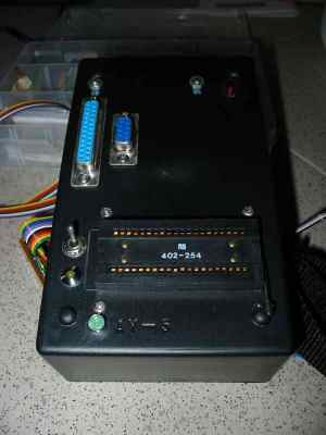
PIC microcontroller Programmer (Completed in the year 2005) My first own build programmer system. Spent quite a lot of time designing and fabricating the plastic box chassis. It works, but I never really work much with it after I brought myself a commercial version. |
|
||||||||||||||||||
|
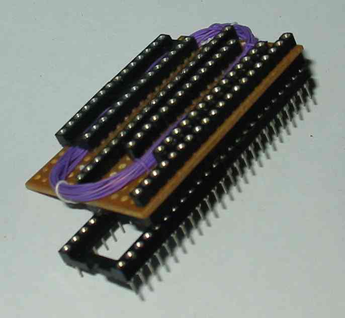
Microcontroller DIP IC Adaptor (Completed in the year 2002-05-xx) This is a interface board for fitting various model of PIC microcontroller to the programmer. The programming pins numer is different for every PIC microcontroller model. This interface board eliminate the need to build a new programmer board for different PIC microcontroller model. |
|
||||||||||||||||||
|
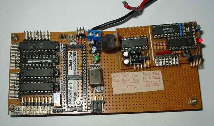
PIC Programmer & Development board (Completed in the year 2002-05-xx) This board is design to be function as a multi purpose PIC microcontroller development board. I have build specially to trial run the microcontroller firmware I wrote. Bi-directional digital buffer are used, to protect the microcontroller from external device during interfacing. After working with microcontroller for some time, I find that this buffer interface is not necessary. Microcontroller I/O ports do not damage easily. When interfacing microcontroller with high powered or unknown devices, opto-coupler can be used instead. Opto-coupler provides maximum isolation as well as protection between the microcontroller and other devices. Attached to the main PCB is a smaller PCB board. It consist of a MAX232 converting computer RS232 to microcontroller TTL serial signal. This small board also include a charge pump circuit that generate 12V from a 5V source for the purpose of programming the PIC microcontroller. This programmer design “Toolkit TK3 PIC programmer” was taken reference from my favourite hobby magazine “Everyday Practical Electronics“. |
Development Board schematic & PCB layout
Programmer Board schematic & PCB layout |
||||||||||||||||||
|
Microcontroller Essential Test Tools (Completed in the year 2002-05-xx) Input switches and Output LED test board interface. It is very useful when doing microcontroller project, because it can help to indicate if the firmware is running correctly inside the microcontroller. A must have kit when doing digital project.
|
|
||||||||||||||||||
|
PIC microcontroller selection references. table updated in 26 May 2007
|


Microchip Microcontroller Common Function Pin Out.
The following table provides a quick overall view the various essential
pins of microchip microcontroller, to allow the use of alternative part
no., and allowing PCB design to suit the most common pin out.
| Specification | ICSP pin out | Vcap pin out | OSC pin out | UART fixed pin out | Preferred I/O use | Comment | ||||||||||||||||
| Microcontroller part no. | Package /Pin no. | Volt | !MCLR | Vdd (+) | Vss (-) | PGD1 | PGC1 | PGD2 | PGC2 | PGD3 | PGC3 | Vcap | DisVreg | OSC1 | OSC2 | TX1 | RX1 | TX2 | RX2 | Input | Output | |
| 64 pins | ||||||||||||||||||||||
| PIC24HJ256GP206A | TQFP/64 | 3V – 3.6V | 7 | 10 19 26 38 57 |
9 20 25 41 |
18 | 17 | 47 | 48 | 16 | 15 | 56 | 39 | 40 | 33 | 34 | 32 | 31 | ||||
| 44 pins | ||||||||||||||||||||||
| PIC24FJ64GA004 | TQFP/44 | 2V – 3.6V | 18 | 17 28 40 |
16 |
21 | 22 | 8 | 9 | 41 | 42 | 7 | 6 | 30 | 31 | EEPROM | ||||||
| PIC24FJ64GA104 | TQFP/44 | 2V – 3.6V | 18 | 17 28 40 |
16 29 39 |
21 | 22 | 8 | 9 | 41 | 42 | 7 | 6 | 30 | 31 | |||||||
| PIC24FJ64GB004 | TQFP/44 | 2V – 3.6V | 18 | 17 28 40 |
16 29 39 |
21 | 22 | 8 | 9 | 19 | 20 | 7 | 6 | 30 | 31 | |||||||
| PIC24F32KA304 | TQFP/44 | 1.8V – 5.5V | 18 | 17 28 40 |
16 29 39 |
21 | 22 | 8 | 9 | 41 | 42 | 7 | 30 | 31 | 3 | 2 | 21 | 22 | ||||
| PIC24FJ32MC104 | TQFP/44 | 3V – 3.6V | 18 | 17 28 40 |
6 16 29 39 |
21 | 22 | 19 | 20 | 33 | 34 | 7 | 30 | 31 | ||||||||
| dsPIC30F2023 | TQFP/44 | 3V – 5.5V | 18 | 7 17 29 40 |
6 17 30 39 |
44 | 1 | 34 | 35 | 41 | 42 | 32 | 33 | 20 | 15 | 34 | 35 | |||||
| dsPIC33FJ128GP804 | TQFP/44 | 3V – 3.6V | 18 | 17 28 40 |
16 29 39 |
21 | 22 | 8 | 9 | 41 | 42 | 7 | 6 | 30 | 31 | No EEPROM | ||||||
| dsPIC33FJ32MC104 | TQFP/44 | 3V – 3.6V | ||||||||||||||||||||
| dsPIC33FJ128MC804 | TQFP/44 | 3V – 3.6V | 18 | 17 28 40 |
6 16 29 39 |
21 | 22 | 8 | 9 | 41 | 42 | 7 | 30 | 31 | ||||||||
| dsPIC33FJ16GS504 | TQFP/44 | 3V – 3.6V | 18 | 17 |
6 16 30 39 |
44 | 1 | 34 | 35 | 41 | 42 | 7 | 32 | 33 | ||||||||
| dsPIC33EP128GM304 | 8x input capture, 12x PWM, 4x UART, 3x SPI, 18x ADC | |||||||||||||||||||||
| Microcontroller part no. | Package /Pin no. | Volt | !MCLR | Vdd (+) | Vss (-) | PGD1 | PGC1 | PGD2 | PGC2 | PGD3 | PGC3 | Vcap | DisVreg | OSC1 | OSC2 | TX1 | RX1 | TX2 | RX2 | Input | Output | |
| 28 pins | ||||||||||||||||||||||
| PIC24F16KL402 | SOIC/28 | 1.8V – 3.6V | 1 | 13 28 |
8 27 |
4 | 5 | 21 | 22 | 14 | 15 | 9 | 10 | 16 | 6 | 4 | 5 | |||||
| PIC24F32KA302 | SOIC/28 | 1.8V – 5.5V | 1 | 13 28 |
8 27 |
4 | 5 | 21 | 22 | 14 | 15 | 9 | 10 | 16 | 6 | 4 | 5 | |||||
| PIC24FJ64GA002 | SOIC/28 | 2V – 3.6V | 1 | 13 28 |
8 27 |
4 | 5 | 21 | 22 | 14 | 15 | 20 | 19 | 9 | 10 | EEPROM | ||||||
| PIC24FJ64GA102 | SOIC/28 | 2V – 3.6V | 1 | 13 28 |
8 27 |
4 | 5 | 21 | 22 | 14 | 15 | 20 | 19 | 9 | 10 | |||||||
| PIC24FJ64GB002 | SOIC/28 | 2V – 3.6V | 1 | 13 28 |
8 27 |
4 | 5 | 21 | 22 | 20 | 19 | 9 | 10 | |||||||||
| PIC24FJ32MC102 | SOIC/28 | 3V – 3.6V | 1 | 13 28 |
19 27 |
4 | 5 | 2 | 3 | 11 | 12 | 20 | 9 | 10 | ||||||||
| dsPIC30F2010 | SOIC/28 | 2.5V – 5.5V | 1 | 13 20 28 |
8 |
17 | 18 | 9 | 10
|
17 | 18 | 11 | 12 | |||||||||
| dsPIC30F2020 | SOIC/28 | 3V – 5.5V | 1 | 13 20 28 |
8 19 27 |
17 | 18 | 11 | 12 | 14 | 15 | 9 | 10 | 17 | 18 | 11 | 12 | |||||
| dsPIC30F2012 | SOIC/28 | 2.5V – 5.5V | 1 | 13 20 28 |
8 19 27 |
17 | 18 | 9 | 10 | 17 | 18 | 11 | 12 | |||||||||
| dsPIC30F3010 | SOIC/28 | 2.5V – 5.5V | 1 | 13 20 28 |
8 19 27 |
17 | 18 | 9 | 10 | 17 | 18 | 11 | 12 | |||||||||
| dsPIC30F3013 | SOIC/28 | 2.5V – 5.5V | 1 | 13 20 28 |
8 19 27 |
17 | 18 | 9 | 10 | 17 | 18 | 21 11 |
22 12 |
|||||||||
| dsPIC30F4012 | SOIC/28 | 2.5V – 5.5V | 1 | 13 20 28 |
8 19 27 |
17 | 18 | 9 | 10 | 17 | 18 | 11 | 12 | |||||||||
| dsPIC33FJ32GP102 | SOIC/28 | 3V – 3.6V | 1 | 13 28 |
8 19 27 |
4 | 5 | 2 | 3 | 11 | 12 | 20 | 9 | 10 | ||||||||
| dsPIC33FJ128GP802 | SOIC/28 | 3V – 3.6V | 1 | 13 28 |
8 19 27 |
4 | 5 | 21 | 22 | 14 | 15 | 20 | 9 | 10 | ||||||||
| dsPIC33FJ128MC802 | SOIC/28 | 3V – 3.6V | 1 | 13 28 |
8 |
4 | 5 | 21 | 22 | 14 | 15 | 20 | 9 | 10 | ||||||||
| dsPIC33FJ09GS302 | SOIC/28 | 3V – 3.6V | 1 | 13 28 |
8 19 27 |
17 | 18 | 11 | 12 | 14 | 15 | 20 | 9 | 10 | ||||||||
| dsPIC33FJ16GS502 | SOIC/28 | 3V – 3.6V | 1 | 13 28 |
8 19 27 |
17 | 18 | 11 | 12 | 14 | 15 | 20 | 9 | 10 | ||||||||
| Microcontroller part no. | Package /Pin no. | Volt | !MCLR | Vdd (+) | Vss (-) | PGD1 | PGC1 | PGD2 | PGC2 | PGD3 | PGC3 | Vcap | DisVreg | OSC1 | OSC2 | TX1 | RX1 | TX2 | RX2 | Input | Output | |
| 20pins | ||||||||||||||||||||||
| dsPIC33FJ12MC201 | Quite mature product. | |||||||||||||||||||||
| PIC16F18344 PIC16F18345 PIC16F18346 |
SSOP/20 |
1.8V – 5.5V | 4 | 1 |
20 |
19 |
18 |
19 |
18 |
***new Same series as PIC16F18325 |
||||||||||||
| 18pins | ||||||||||||||||||||||
| dsPIC30F3012 | SOIC/18 | 2.5V – 5.5V | 1 | 14, 18 |
13, 17 | 11 | 12 | 6 | 7 | 11 | 12 | Mid number of I/O, operating at 5V. | ||||||||||
| 14pins | ||||||||||||||||||||||
| PIC24F04KA200 | TSSOP/14 | 1.8V – 3.6V | 1 | 14 | 13 | 3 | 2 | 6 | 7 | 4 | 5 | 11 | 12 | 10 | EEPROM (Don’t use this in future. Use alternative PIC16F1825) |
|||||||
| PIC24F08KL200 | TSSOP/14 | 1.8V – 3.6V | 1 | 14 | 13 | 3 | 2 | 6 | 7 | 4 | 5 | 11 | 12 | 10 | Compatiable to PIC24F04KA200, with more memory. (Don’t use this in future. Having problem using the I/O pins as input (RA4, RB4, RA2, RA3), no access to AD1PCFG to enable digital input. Use alternative PIC16F1825) |
|||||||
| PIC16F1825 | TSSOP/14 | 1.8V – 5.5V |
4 |
1 |
14 |
13 |
12 |
2 |
3 |
13 |
12 |
6 |
5 |
Wide
voltage range for a middle size chip. 12x I/O pins. Internal weak
pull-up don’t work too well as voltage starts to drop when too many
pull-up gets loaded (better design with external pull up). Not suitable for high speed signal processing (for <10us switching speed). |
||||||||
| PIC16F18323 PIC16F18324 PIC16F18325 PIC16F18326 |
TSSOP/14 | 1.8V – 5.5V | 4 | 1 | 14 | 13 | 12 | 13 | 12 | ***new – EEPROM Same series as PIC16F18345 |
||||||||||||
| 8 pins | ||||||||||||||||||||||
| PIC16F18313 |
SOIC/8 | 1.8V – 5.5V | 4 | 1 | 8 | 7 | 6 | 2 | 3 | 7 |
6 | compatiable to the 16F1832x, 34x series SOIC footprint. | ||||||||||
| PIC12F1840 (consider using cheaper PIC16F18313) |
SOIC/8 | 1.8V – 5.5V | 4 | 1 | 8 | 7 | 6 | 2 | 3 | 7 |
6 | UART | ||||||||||
| PIC12F1822 | SOIC/8 | 1.8V – 5.5V | 4 | 1 | 8 | 7 | 6 | 2 | 3 | 7 | 6 | UART | ||||||||||
| PIC12HV615 | SOIC/8 | 2-15V | 4 | 1 | 8 | 7 | 6 | 2 | 3 | 2-15V | ||||||||||||
| PIC12F508 | SOIC/8 | 2-5.5V | 4 | 1 | 8 | 7 | 6 | 2 | 3 | low cost | ||||||||||||
| Microcontroller part no. | Package /Pin no. | Volt | !MCLR | Vdd (+) | Vss (-) | PGD1 | PGC1 | PGD2 | PGC2 | PGD3 | PGC3 | Vcap | DisVreg | OSC1 | OSC2 | TX1 | RX1 | TX2 | RX2 | Input | Output | |
| 6 pins | ||||||||||||||||||||||
| PIC10F322 | SOT23/6 | 1.8V – 5.5V | 6 | 5 | 2 | 1 | 3 | 3 | 4, 6 | 1, 3 | most powerful | |||||||||||
| PIC10F200 | SOT23/6 | 2V – 5.5V | 6 | 5 | 2 | 1 | 3 | 4, 6 | 1, 3 | low cost | ||||||||||||
Legend
Product Identification System (example)
dsPIC 33 FJ 16 MC1 02 T E / SP – XXX
—– — — — — — – – — —
1 2 3 4 5 6 7 8 9 10
1 – Microchip Trademark
2 – Architecture
10 –
12 –
16 –
18 –
24 – 16-bit Microcontroller
30 –
33 – 16-bit Digital Signal Controller
3 – Flash Memory Family
FJ – Flash program memory, 3.3V
F – Flash
EP – Enhanced Performance
HJ – Flash program memory, 3.3V, High-speed
4 – Program Memory Size (Kbyte)
5 – Product Group
GP? – General Purpose family
MC1 – Motor Control family
GS? – Switch Mode Power Supply (SMPS) family
6 – Pin Count
01 – 18-pin and 20-pin
02 – 28-pin and 32-pin
04 – 44-pin
06 – 64-pin
10 – 100-pin
7 – Tape and Reel Flag
– Standard packaging (tube or tray)
T – Tape and Reel
8 – Temperature Range
I – -40ºC to +85ºC (Industrial)
E – -40ºC to +125ºC (Extended)
H – -40ºC to +150ºC (High)
9 – Package
P – PDIP (Plastic Dual In-Line)
SS – SSOP (Plastic Shrink Small Outline)
SP – SPDIP (Shinny Plastic Dual In-Line)
SO – SOIC (Plastic Small Outline)
SN – SOIC (8-Lead)
SL – SOIC
ML – QFN (Plastic Quad, No Lead)
MR – QFN (Thin Quad Flatpack)
MG – QFN (Micro Lead Frame)
MM – QFN-S (Plastic Quad, No Lead)
MV – UQFN
PT – TQFP (Plastic Thin Quad Flatpack)
PF – TQFP (Plastic Thin Quad Flatpack, 14x14mm)
ST – TSSOP
TL – VTLA (Very Thin Leadless Array)
MF – Micro Lead Frame (DFN)
MC – DFN
OT – SOT-23
10- Pattern
QTP, SQTP, Code or Special Requirements
It is a headache trying to maximise the pin compatibility with a wider range of microcontrollers and applications,
such that firmware changes can be minimised.
The following are suggesting pins use for reference, base on the following microcontroller:
| Microcontroller part no. | Package /Pin no. | Volt | !MCLR | Vdd (+) | Vss (-) | PGD | PGC | OSC1 | OSC2 | TX1 | RX1 | TX1 Ctrl |
TX2 | RX2 | TX2 Ctrl |
Output Indicators |
Input Switch |
Input Analog |
I/O | PWM | ||||
| 44 pins | ||||||||||||||||||||||||
| PIC24FJ64GA002 | TQFP/44 | 2V – 3.6V | 18 | 17 28 40 |
16 |
21 | 22 | 30 | 31 | 44 | 1 | 3 | 8 | 9 | 10 | 33, 34, 41 | 21, 22 | 19,20 | 15, 14, 11, 10 | |||||
| PIC24FJ64GA002 | SOIC/28 | 2V – 3.6V | 1 | 13 28 |
8 27 |
4 | 5 | 9 | 10 | 17 | 18 | 16 | 21 11 |
22 12 |
23 | 11, 12, 14 | 4, 5 | 2,3 | 26, 25, 24, 23 | |||||
| PIC12F1840 | 4 | 1 | 8 | 7 | 6 | 2 | 3 | 7 | 6 | 7, 6 | 4, 7, 6 | 3, 5 | ||||||||||||
| PIC10F322 | 6 | 5 | 2 | 1 | 3 | 1, 3 | 6, 1, 3 | 1, 3, 4 | 4 | 1, 3 |

Singapore Customized, custom made Electronics Circuits & Kits
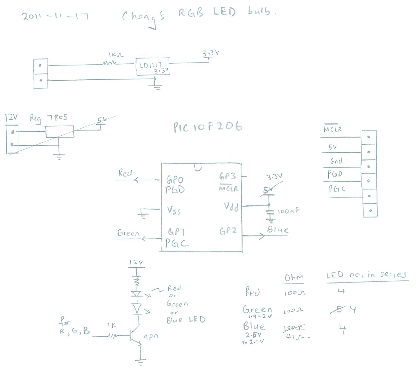
PIC10F206 Microcontroller Schematic source code:
|
 |


| Microchip MPLAB microcontroller startup troubleshooting
guide. 2009-10-08 Getting my “hello world” firmware loaded into my new hardware design pose the most difficult part of the process. Time consuming doing debugging, and it can takes from half a day to two. The most difficult part, to spent those precious engineering time in debugging. Debugging what I thought I should be good in since I have done so many microcontroller project. Till this day, I still have the problem every time I start microcontroller project after a few months break. The reason I have this guide written. To provide myself possible solution, that can help me, if I encounter the same issue again.
|
|
Setting up the environment for project using MPLAB v8.70 1) Create a project folder. Open the MPLAB IDE software. 2) Open a new Project. Project>New… and enter in a name for the project. 3) Select the microcontroller that is use in the project. Configure>Select Device… and select the microcontroller for your project. 4) Check the configuration mode ‘Release’. Project>Build Configuration>Release 5) Select the correct toolsuite for your project. Project>Select Language Toolsuite… for typical C lanaguage implementation, choose “MPLAB” C30 C Complier (pic-30-gcc.exe) v3.24 6) Add in the search path for your microcontroller’s header file. Project>Build Options…>Project>Directories>Include Search Path, choose add to add in the directory that contains the microcontroller’s header files. For my example, the header is located in the directory “C:\Program Files (x86)\Microchip\MPLAB C30\support\dsPIC33F\h” 7) Add in or create all the *.c & *.h files, to start your programming.
|
|
| I use PICkit2 most of the time, because it is a small and
compact programmer. Today, I tried out PICkit3. Well I am quite impress with
the changes from PICkit2. I hope to get that one day. As for this article,
the error messages is meant for PICkit2 use on the IDE Mplab version 8.36. I do not have much problem doing the compilation of my C programs. The frustration comes during the loading of my hex codes into my newly design prototype circuit. Most of the time is due to human error, because my prototype board are mainly hand soldered, pin by pin. On the left is the typical error message I encounter. I am scare of them to be frank. I see them almost every time.
|
Initialisation of PICkit2 when connected to
Mplab Initializing PICkit 2 version 0.0.3.63 |
| Every time when I press the shortcut key Alt+G,
G to program the controller, PICkit will attempt to read the device ID of
the microcontroller. The microcontroller used in this example is
PIC24FJ32GA004. As you can see in the error on the right. PICkit is expecting the microcontroller with device ID 0x44D0000. The read by PICkit detects a ID of 0x0. In fact this same error is identical as if the PICkit programmer is not inserted to the ICSP programming pins at all. This is a hard evident that the microcontroller is not wired properly or evenly not wired at all.
|
Error Encounter using PICkit2 version 2.63,
MPLAB version 8.36 Programming Target (10/8/2009 4:37:06 PM)
|
|
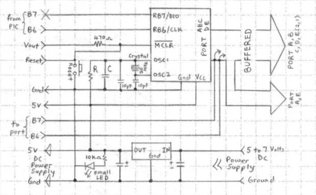
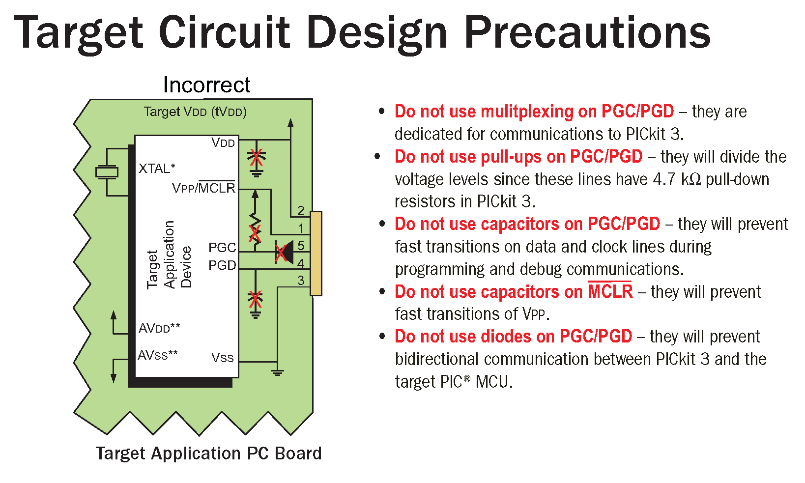
1) The first thing to check if your hardware. It is most of the time the source of the problem. Check if the ICSP programming pins are wired correctly ICSP pin out Pin 1: !MCLR Pin 2: Vdd (3.3V or 5V, depends on the device) Pin 3: Vss (ground) Pin 4: PGD (data line) Pin 5: PGC (clocking line) Pin 6: unused
Attached on the left is the basic schematic of the microcontroller PIC24FJ32GA004 if your wiring is exactly the same as what is shown, PICkit2 should be able to load the hex file into your controller without any problem. An advise to you, don’t assume that your wiring is correct. Check 2 or more times to ensure. This is often one of my major mistake make. The schematic is typically correct, but because of the confident doing many similar project, the checking is often the lacking part. For PIC24FJ series controller, there is a pin Vcap & DISVREG. Make sure that there is the capacitor there. !MCLR pin to be pull up to Vdd using a resistor about 10kohm. The following pins are to be connected to PIC24FJ32GA004, in order for the ICSP programmer to download the *.hex files onto the microcontroller. Improper connection will definitely generate programming error messages.
Pins connection Pin 18
connect to !MCLR
|
Socket holder for PIC24FJ32GA004 TQFP-44
prototype board
TQFP-44 Prototype board or adaptor This sub-board adaptor helps to convert small smd components to 2.54mm pitch for mounting onto pcb. The larger 2.54mm pitch will be easier to work with when doing prototyping. The board is available from PIC-CONTROL part no. PIC-200
|
|
2) Check if the header file declare in the source code is correct This actually informs the PICkit programmer what type of device it is going to encounter. This is also why the error message indicates the expected ID of 0x44D0000, which is the device ID for PIC24FJ32GA004 microcontroller. Some example of other device ID for PIC24FJ series microcontroller. Microcontroller Device ID PIC24FJ16GA002 0x00444 PIC24FJ32GA002 0x00445 PIC24FJ48GA002 0x004466 PIC24FJ64GA002 0x00447 PIC24FJ16GA004 0x0044C PIC24FJ32GA004 0x0044D PIC24FJ48GA004 0x0044E PIC24FJ64GA004 0x0044F You might double check if the microcontroller device is selected correctly under the menu “Configure”. It is probably not necessary as the device select is base on what is written with your source code.
|
|
| 3) Check if you have included the correct linker file for the microcontroller
PIC24FJ32GA004. The file name goes something like this, “p24FJ32GA004.gld”.
The file is available under the C30 folder “C:\Program Files\Microchip\MPLAB
C30\support\PIC24F\gld”, after you installed the C30 compiler
for your Mplab.
|
|
| 4) Do not solder capacitors on PGD, PGC pins. PGD PGC can be use for programming
as well as I/O during operation. Due to the programming use, I will usually
design this pin as an input during operational. This feature do free up the
controller pins for other uses. Using it as an input, it does not have any load
to worry about. There is one time I added capacitor across the input and ground,
thinking that it may filter any switching noise from the switch input. The
capacitor turns out to cause problem to the PGD PGC pins. It results in a slow
slew rate causing data error during program loading.
|
Check out the following notes when designing ICSP on your microchip microcontroller.
|
| 5) Ensure that your circuit is powered from it’s own power source. This is
especially needed if you have a big load of components on our board. The PICkit
programmer might not be able to support all those power. Sometimes the PICkit
doesn’t provide the power. There should be a settings that allows your PICkit to
supply the power.
|
|
| Another similar error occur. This time round, the device ID is read as 0xFFFF0000. I found the problem and it happens that the ICSP pin 4 (PGD, data) and pin 5 (PGC, clock) has been wire wrongly. They are swapped. | Programming Target
(10/8/2009 6:13:18 PM) PKWarn0003: Unexpected device ID: Please verify that a PIC24FJ32GA004 is correctly installed in the application. (Expected ID = 0x44D0000, ID Read = 0xFFFF0000) Erasing Target Programming Program Memory (0x0 – 0x23FF) PE Error: Using ICSP Verifying Program Memory (0x0 – 0x23FF) PE Error: Using ICSP PK2Error0027: Failed verify (Address = 0x0 – Expected Value 0x40200 – Value Read 0xFFFFFF)
|
| When the PICkit2 has sucessfully loaded the hex file into the microcontroller chip, you should see the message on the right. | PICkit2 program loaded into microcontroller
sucessfully Programming Target (10/9/2009 10:30:46 AM) |
 Front
Front Back
Back

| Error Message Encountered | Solution: |
Error encountered while loading codes onto the chip: “You are trying to change protected boot and secure memory. In order to do this you must select the “Boot, Secure and General Segments” option on the debug tool Secure Segment properties page. Failed to program device” |
To program a chip that is code protected, need to set PICkit3 into a special mode. Try re-program the chip again. The new code should be able to over-write the old codes on the chip. Alternative old solution method: |
| Useful C30 compiler pre-processor | |
#define FIRMWARE_DATED __DATE__ //microcontroller dsPIC33FJ128GP804 #define CRYSTAL_MHZ 8 #define XBEE_BAUDRATE _115200bps #define NUM_OF_LOADCELL 4 //Features Check #warning Testing only //print warning message during compile time //Useful symbols which can be use to load the file name, code line and date of the code compilation
|
| Useful C30 codes | |
Important, what to put in a header *.h.macro definitions (preprocessor #defines) |
|
| Configuration Settings Reference |
PIC18 Configuration Settings Addendum, 51537a.pdf Configuration bits generator. 1) Open MPLABx, go to Window > PIC Memory views > Configuration Bits 2) A Configuration Bits section will be shown. Setup the configuration bits accordingly. 3) After the setting is done, click on the button “Generate Source Code to Output” 4) Copy and paste the configuration code to your source code. |
| List of interrupts |
For XC8 void __interrupt(high_priority) Interrupt_ISR()
For XC16 void __attribute__((__interrupt__, __shadow__, __auto_psv__)) _DefaultInterrupt(void) Note: Be careful when implementing the “DefaultInterrupt”, as all interrupt vector may point to this rountine. (2016-02-05)
void __attribute__((__interrupt__,auto_psv,__shadow__)) _U1RXInterrupt(void) void __attribute__((__interrupt__, __shadow__, __auto_psv__)) _IC1Interrupt() //input capture interrupt void __attribute__((__interrupt__, __shadow__, __auto_psv__)) _T1Interrupt(void) //timer 1 interrupt void __attribute__((__interrupt__, __shadow__, __auto_psv__)) _SPI1Interrupt(void);
|
Data type structure. Useful in creating access for data bits, byte or word. This helps saves memory space and data handling codes. |
//Settings for individual channel #define NUMOFCHANNEL 8 typedef union //Accessing data on the Data structure ———————————————————– //another example of a data type structure typedef union //accessing the data structure
———————————————————– typedef union ———————————————————– typedef union // readingXXX.reading[0] = 0x00000123; //print seq 00 00 01 23 00 00 45 67 00 00 89 AB 00 00 CD EF }DATAREADING; ———————————————————– //Complex data union, data struct example typedef enum ———————————————————–
|
| enum | Example1 of how to use enum. (see better example2) Create a header file for Enum “Enum.h”, and place the following enum defintion, enum BOOLEAN ————————————————————– For each of the *.c file that you want to use the enum BOOLEAN, include the header file “Enum.h”. 1) declare a enum variable 2) declare a function ————————————————————– For header *.h file that you want to use the enum BOOLEAN, extern enum BOOLEAN; #################################################################################### Example2 of how to use enum. (betterexample) Create a header file for Enum “Enum.h”, and place the following enum defintion,typedef enum ————————————————————– For each of the *.c file that you want to use the enum BOOLEAN, include the header file “Enum.h”. 1) declare a enum variable 2) declare a function ————————————————————– For header *.h file that you want to use the enum BOOLEAN, (have problem here with enum. Prototype declare in the header cannot have the enum as data type.) BOOLEAN isDone(); |
|
enum PORTIN enum LED_MODE enum EDGE //define enum type “EDGE” //declare a variable “myEdgeVar” of type EDGE EDGE myFunction(EDGE myVar) { } |
|
void initOscillator() #ifdef dsPIC33FJ256GP506A CLKDIVbits.PLLPOST = 0b00; // N1=2 //PLL module, Fosc = Fin*(M/(N1*N2)) //PLLPRE==2, PLLPOST==0, PLLDIV==78 //PLLDIV==37 } //************************************************* //define RPxx pin number=outputPin Function //Output Peripheral pin /* #ifdef ETHERNET_COMMUNICATION //map UART2 pins //map SPI1 pins //config for input capture //__builtin_write_OSCCONL(OSCCON | 0x40); |
|
| Clock frequency defination |
FOSC – clock frequency (final system clock frequency) FCY – instruction cycle clock (usually = 1/2 FOSC) FP – clock frequency source to peripherals (usually = FCY) |
| Pointer to function. (Callback function) Callback structured the *.c file such that they provide services and not access another *.c for services. *.c calling each other can make the code very messy. Service providing class providing services and allow callback will means that calling of functions will allows be from the other class, and not the service providing class. The example on the right shows a timer interrupt service. Other classes that need to use this interrupt class will register itself and waiting to get called from the registered callback. This means that the interrupt class coding can be written in a generic manner without referencing or calling other classes. |
void
(*timer1Callback)();
//declare variable for function callback //register the function for timer callback void registerTimer1CallBack(void (*f)()) { initTimer1(); timer1Callback = f; } void __attribute__((__interrupt__, __shadow__, __auto_psv__)) _T1Interrupt(void) //timer 1 interrupt { if(timer1Callback != NULL) (*timer1Callback)(); //call the registered function. IFS0bits.T1IF=0; } void initTimer1(void) { T1CONbits.TCKPS=0b11; //1:256 T1CONbits.TCS=0; T1CONbits.TGATE=0; //disable TGATE T1CONbits.TSYNC=0; //does not sync with external clock input T1CONbits.TSIDL=0; //continue in idle mode //PR1=0x023F; //set period for timer (set to 10ms timer interrupt) PR1=0x0039; //set period for timer (set to 1ms timer interrupt) //set timer interrupt priority to level 1 IPC0bits.T1IP=1; //clear timer interrupt flag T3IF bit IFS0bits.T1IF=0; //enable timer3 interrupt IEC0bits.T1IE=1; //starts the timer T1CONbits.TON=1; } //———————————————————– //from another file doing the registration for interrupt to callback #define RUN_TIMER_COUNT 100 void initRunTimer() { registerTimer1CallBack(timer1msCallBack); //function registrating a function which can be call back from the interrupt function. } void timer1msCallBack() { //interrupt at 1ms interval static int runTimerCount = RUN_TIMER_COUNT; runTimerCount–; if(runTimerCount<=0) { runTimerCount = RUN_TIMER_COUNT; indicatorToggle(RUN); } } |
| Accessing PORTB bits dynamically |
Quoted from http://tutor.al-williams.com/pic-detail2.html “ First, the I/O pins are tied to the PORT registers, as you’d probably guess. However, on reset, all port pins are set to inputs. If you want to use a port pin as an output, you’ll need to change the corresponding direction bit from a 1 (the default) to a 0. So to prepare PORTB pin 0 for output you might write: bsf status,rp0 ; rp0=1 - select bank 1 It is good practice to reset the bank to 0 as soon as you are done accessing another bank. So then if you wanted to set the output to 1 you might write: bsf portb,0 The other quirky behavior is the interaction between INDF and FSR. INDF isn’t like an ordinary register. Instead, it mirrors another register indicated by the address in FSR. For example, location 0x6 is the PORTB register. Suppose you write: movlw 6 ; W=6 Now the INDF register is really an alias for PORTB. So you might write: bsf indf,0 ; set bit 0 This instruction doesn’t really set bit 0 of INDF, it sets bit 0 of PORTB. Since FSR is an 8-bit register, it can contain a complete address from bank 0 or bank 1 (just treat bank 1 addresses as ranging from 0x80-0xFF). To access bank 3 and and bank 4 using FSR/INDF, you have to set the IRP bit in the STATUS register. RP0 and RP1 don’t apply to INDF access! “ |
| Preserving stack memory using inline |
void main(); inline void init(); inline void loop(); void main() { initPinMapping(); //peripheral pin select getResetType(); init(); INTCONbits.PEIE = 1; //enable peripheral interrupt INTCONbits.GIE = 1; //enable global interrupt while(1) { loop(); } } inline void init() { initIndicator(); initProtocol(); initAudioIn(); } inline void loop() { } |
| Microchip software reset function |
for XC16 compiler asm(“RESET”); for XC30 compiler Reset(); |
| Watchdog function |
for XC30 compiler ClrWdt(); |

Singapore Customized, custom made Electronics Circuits & Kits
| Crystal Selection for Microcontroller’s UART | ||||
| 2014-03-08
Today I realised something about the UART in microcontroller that I am
not aware about, even many years of firmware programming. I was
troubleshooting the UART in my microcontroller. The data that are sent
or received are corrupted. The first char is always received correct. I
realised that it could be that the microcontroller baud rate is having
the problem. I have been using this 8MHz crystal for many of the
project, but this time the data corruption is too serious to be
ignored. I was using PIC24FJ64GA004 microcontroller. From the UART peripheral datasheet (DS70000582E), I managed to recompute the baud rate and its error. The error is too high. I have no idea why that baud rate was peviously selected. UxBRG = (Fp / (4 x Baud Rate)) – 1 Calculated Baud Rate = Fp / (4 x (UxBRG + 1)) Error = (Calculated Baud Rate – Desired Baud Rate) / Desired Baud Rate x 100% I wanted to find out which clock frequency can provide the least error. To speed up the computation, I have create a spreadsheet using OpenOffice Calc (similar to excel spreadsheet). 2014-03-08_baudrate_computation_microchip.ods When I try to input the other common crystal that I have on hand, I realised 7.3728MHz is computed to have an error of 0%. It is a perfect score. This makes me curious to find out more other crystal that is able to provide a 0% error for UART. It turns out that those crystal that have a multiple of 2400, will be able to provide the UART with a 0% error. The 2400 figure comes from one of the commonly use RS232 baud rate 2400bps which is the common denominator for all the commonly used baud rate. Crystal that have a frequency that is multiple of 2400 will be the best for the UART peripheral. The following provides the commonly available crystal frequency that is suitable for UART peripheral operation.
|
Keyword: Microchip PIC microcontroller prototype development, PIC programmer, Max232, ICSP programming interface, output buffer, LED indicator, 74LS595 74HC595, 74LS244 74HC244, DC-DC power supply, 40pins 28pins 18pins DIP IC
PIC18F4550, PIC18F452, PIC16F877a
PIC18F252, PIC16F876a
PIC16F88, PIC16F628a, PIC16F84a