Edited by Lim Siong Boon, last dated 06-May-09.
Short cut to your reference guides and charts
| 1. Introduction to SMD soldering | |||||||||||||||||||||||||||||||||||||||||||||
|
SMD IC stands for surface mount device integrated circuit, or commonly known
as SMT surface mount technology. Why go into SMD? Small in size, light in
weight. This is the advantage of smd. Being small, engineer is able to
design small electronics gadget that people can carry around. It is quite
obvious that people prefer small mobile phone. The ultimate advantage will be lower cost to consumer. Being small in size, the printed circuit board (pcb) can be small, meaning low cost. Transportation cost can be reduce because it is now lighter and more products can be packed into the same box. Space required is less, meaning cost saving on the warehouse storage. PCB board is easy to route without the through hole. Better signal integrity. Easily assembled by machine. There is too much advantages. Going SMT is certainly the way forward. |
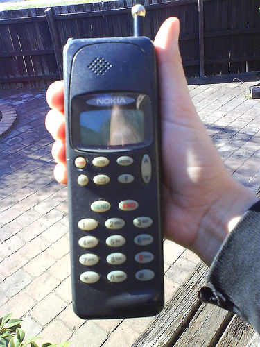
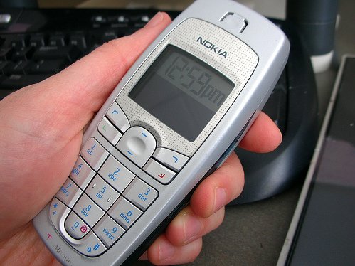
Technology evolution, from big
to small.
Smaller mobile phone
Even smaller phone
|
||||||||||||||||||||||||||||||||||||||||||||
|
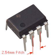
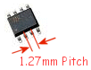
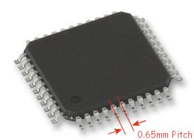
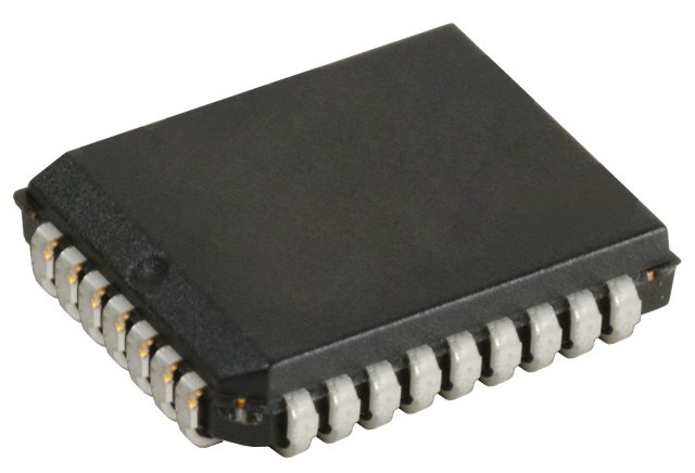
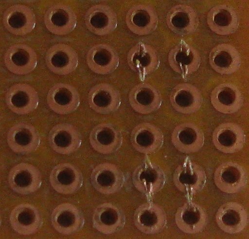
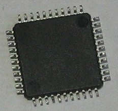
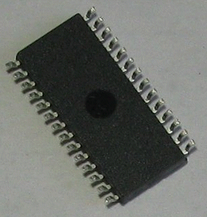
I used to build circuits using dual in-line package (DIP or DIL) IC only. I hardly thought of using surface mount device/component (SMD) because I have great doubt that I can solder the fine legs of the IC chip. The pitch for the older DIP IC package are 2.54mm. Pitch is the distance between adjacent pins as illustrated in the picture. Most IC comes with a variety of packages. The IC that I know of, offer both the SMD and DIP packages. I thought that I will never ever need to use smd packages until one day, I have no more choice. I managed to pick up new circuit designs, and discover more and more new IC chips. Most new IC chips design do not have DIP packages. You can hardly find one. I realised that in order to implement better circuits, I need to learn to use new IC chip. In order to use the new chip, I have to find ways to solder smd components. That’s where I venture into the world of smd. Nowadays people prefer to use smd, because they are small in size, which turns out to be cost efficient fabricating small PCB. With smaller PCB, space & weight is saved, resulting in lower cost for the transportation/distribution and storage. Research and research, I got to know from other electronics guru that smd is in fact easier to work with than through hole. I try it out and from that day onwards, I am in love with smd components. Small to solder, but it save me the effort to cut the lead for through hole component. I managed to store my component using minimum box and space. There are many many advantage to work with smd. Many people might think that you need special tools like a rework station or fine tip iron to solder the small smd components with small pitches. With the correct technique, you can use your soldering iron to do the soldering. In fact my 60W goot TQ-95 soldering iron has quite blunt tip. So thick that most people think that it is not possible to solder smd IC with fine pitches. Fine tip iron is easy to reach the fine lead, but I find that it is not as hot as the same iron with blunt tip. If you prefer fine tip, I will recommend hotter soldering iron or those which can allow you to adjust the temperature, they can be hot. I managed to solder smd package TQFP, SSOP QSOP with pitch as small as 0.5mm. Width of the lead of about 0.3mm. Dealing with SMD components do not necessary requires you to fabricate a professional pcb board. You can also mount smd components on low cost prototyping board. To start off implementing smd components, you might like to try using the soic package. Quite common at this point in time, but may just phase out as what has happened to the dip packaging. SOIC has a pitch of 1.27mm, which is exactly half of DIP packages. This size is great because I can solder the IC to the same old 2.54mm pitch prototyping donut padded board. What I usually do is to cut the donut pad into half. Soldered onto each pad is two pins 1.27mm apart. You can refer to the following article, for further illustration. |
Through hole packages
SMD packages
|
||||||||||||||||||||||||||||||||||||||||||||
|
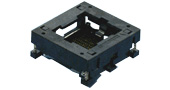
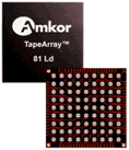
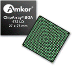
With so much advantage there is indeed a disavantage. SMD IC comes with many type of packages with different pitches. Unlike DIP IC, the pitch is typical 2.54mm. I can easy purchase a prototype board with 2.54mm, and almost all the DIP will fit to the board. SOIC package can still be mounted onto the 2.54mm prototype board. The rest of the SMD IC chip has quite a wide range of completely different packaging. This make them difficult to start with, without having to fabricate a PCB. There are actually solution to this. Most IC company usually introduce their IC chip together with a prototype board for the IC. Another solution will be to use a pre-fabricated prototyping board that allows mounting of various smd footprint. You can search for the various names such as – prototype adaptor – chip adaptor – smd prototyping board – smd to dip adaptor – smd socket – smd adaptor – smd to 2.54mm converter – SMD to DIP converter – chip carrier You can refer to the following article, for further illustration. |
Various distributor for the prototyping adaptor
|
||||||||||||||||||||||||||||||||||||||||||||
|
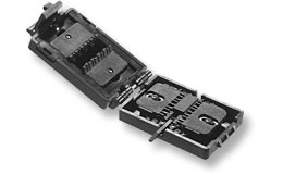
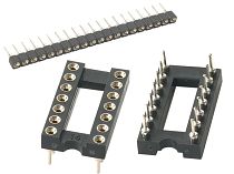
In prototyping with DIL IC, pcb mount IC socket is usually used, so that the IC can be removed easily if damaged. Some sockets are designed for programming used where the chip can be inserted and remove easily for programming purpose. To remove the component, you need not have to do de-soldering. Like DIL package, smd also comes with their own IC socket. There are many variety of smd packaging, and getting the socket for your smd components is not going to come cheap & easy compare to DIL. Therefore I usually built prototype without any sockets for smd design. After numerous attempts designing and building of circuits, you will definitely attain a certain level of confident on your design without considering IC socket. Without the socket, cost and space are saved significantly. SMD IC sockets:
|
DIL IC sockets/ holder. Turn pins designs is of better quality.
Various distributor for SMD socket
|
||||||||||||||||||||||||||||||||||||||||||||
|
The headache
will come when you really need to removed the smd IC. How do you remove the
IC from the PCB? For de-soldering of smd component more than 3 leads, you
can add in more solder to connect up the IC pins heat pins on all the sides
of the IC and eventually pull out
the component. It is easier to use the rework station or IR heater to de-solder smd
components. The rework station uses hot sir to melt down the solder on the
board. You will need to aim the hot air at the solder joint.
If you do not have the lurxy of getting the rework station, another possible method might be to use a special solder that has lower melting point. LowMelt® DeSolder Wire. A lower melting point means that the solder will takes a longer time to cool down to a solid. This allows you more time to remove the IC after heating up the solder. The solder is flooded onto the pins of the IC. The pins are heated up together using a soldering iron and the smd IC can then be removed easily with a tweezer. Low melt solder wire
|
|
 A
phone small enough to carry around.
A
phone small enough to carry around.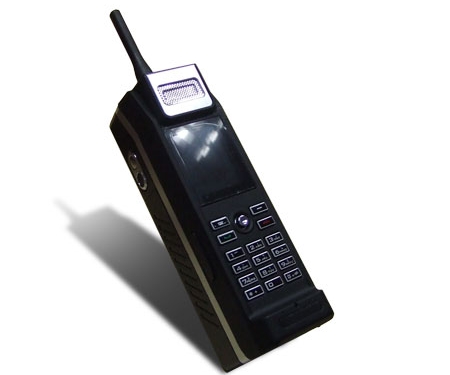
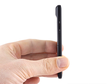
 Mobile
phone as thin as biscuit.
Mobile
phone as thin as biscuit.


 Rework Station


Singapore Customized, custom made Electronics Circuits & Kits
 The prototype board above has pad with 2.54mm pitch and is designed for DIL and through hole components. The board is easily available from local store. Dealing with smd components on this 2.54mm pitch board is not difficult as well. I have been using this board to solder quite a number of surface mount components. – SOIC – DPAK – SOT23-6, SOT-3 – TO-263 – PSOP
|
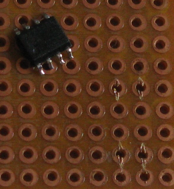
High pin count component with pitch less than 1.27mm will not be suitable to mount onto this board. For passive smd component like resistor, capacitor or inductor which only have 2 pin, mounting is simpler. Size is not an issue soldering onto the board. |
|
Align the SMD IC to the position on the pad. Mark out the pad for the
cutting to be done. Use a penknife to cut the donut pad into half. Ensure that the half pad does not short circuit using your multi-meter. Sometimes the cut may not be deep enough or conductive reside between the gap resulting in a short circuit. Remember to ensure that each is proper cut before you start to solder. Align the smd with your finger or tweezer and begin soldering one of the pin. Check if the IC is still properly align after soldering the first pin. If not, heat up the soldered pin and realign again. After the ICis align, solder all the rest of the pin. If the solder bridge across to the adjacent pin, use a soldering sucker to remove the excess solder. The cut between the pad usually make the solder harder to bridge across the adjacent pin. Bridging is still possible, and it is quite easy to have it removed.
|
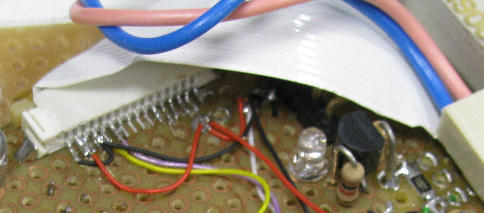 SMD ribbon cable connector being soldered onto the 2.54mm pitch prototype board. |
Example of building the circuit using surface mount component on the prototyping board with 2.54mm pitch pads. As shown above, the pins are being wired by fine wire wrapping wire. The single core wire is very flexible and comes in a variety of color, making it easy to identify the type of signal being carried by the wire. |


|
3. SMD soldering (prototyping PCB socket 2.54mm pitch)
|
||||||||||||||||
|
What you need…
|
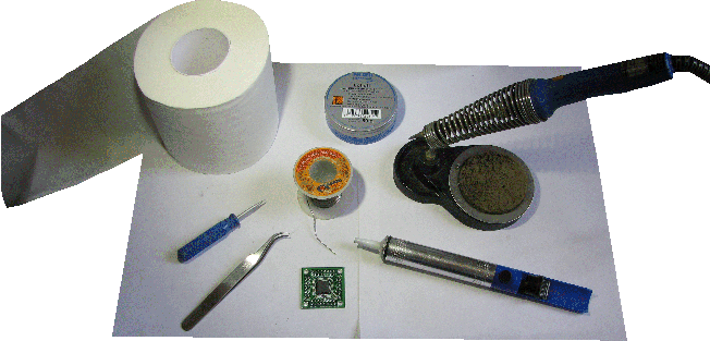
List of items: – Surface IC chip (TQFP package) – Surface mount IC adaptor or converter – Soldering Iron – Tweezer or Pincer – Solder with flux core – Soldering Flux – Stick for coating flux – Wiping paper – Tinner
|
|||||||||||||||
|
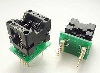
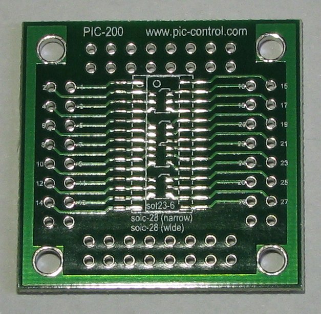
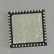
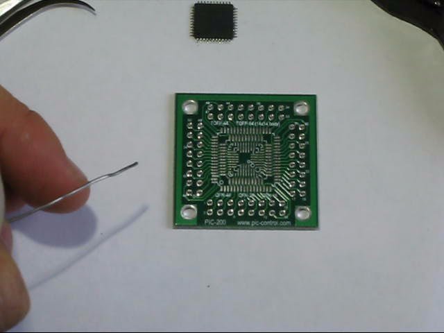
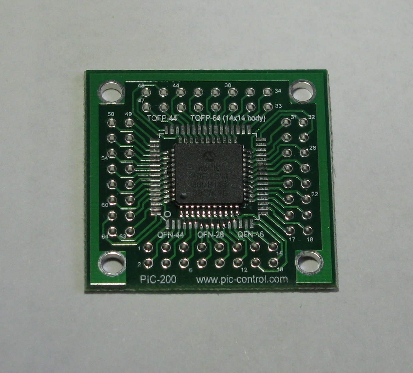
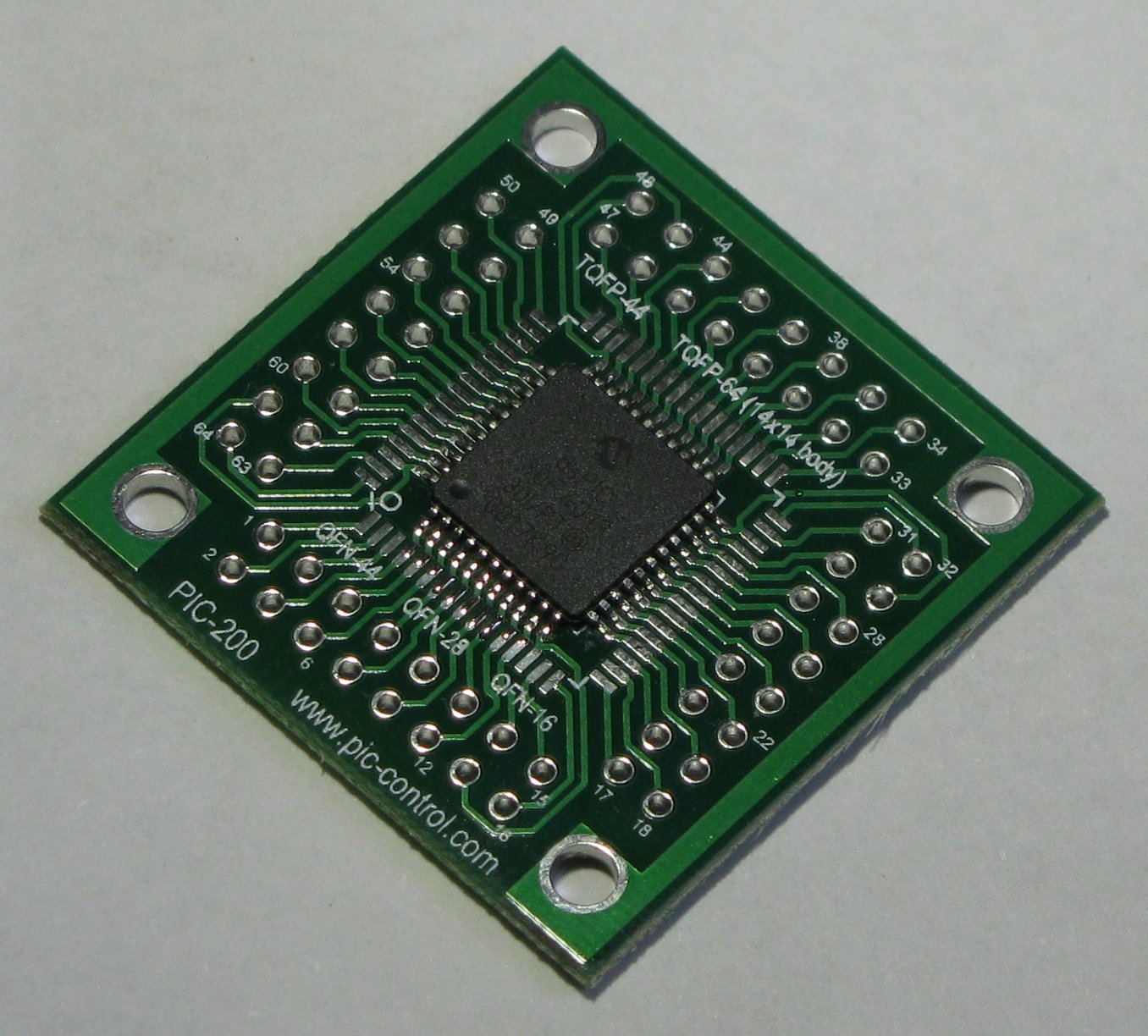
PIC-200 smd to 2.54mm pitch adaptor from
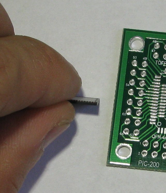
Holding onto the side view of the QFN package IC.
|
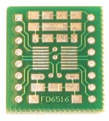
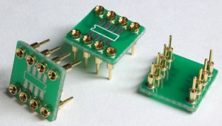
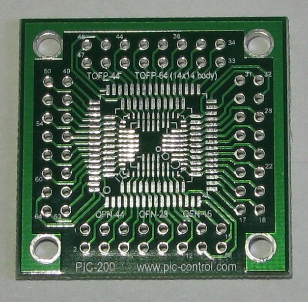
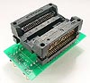
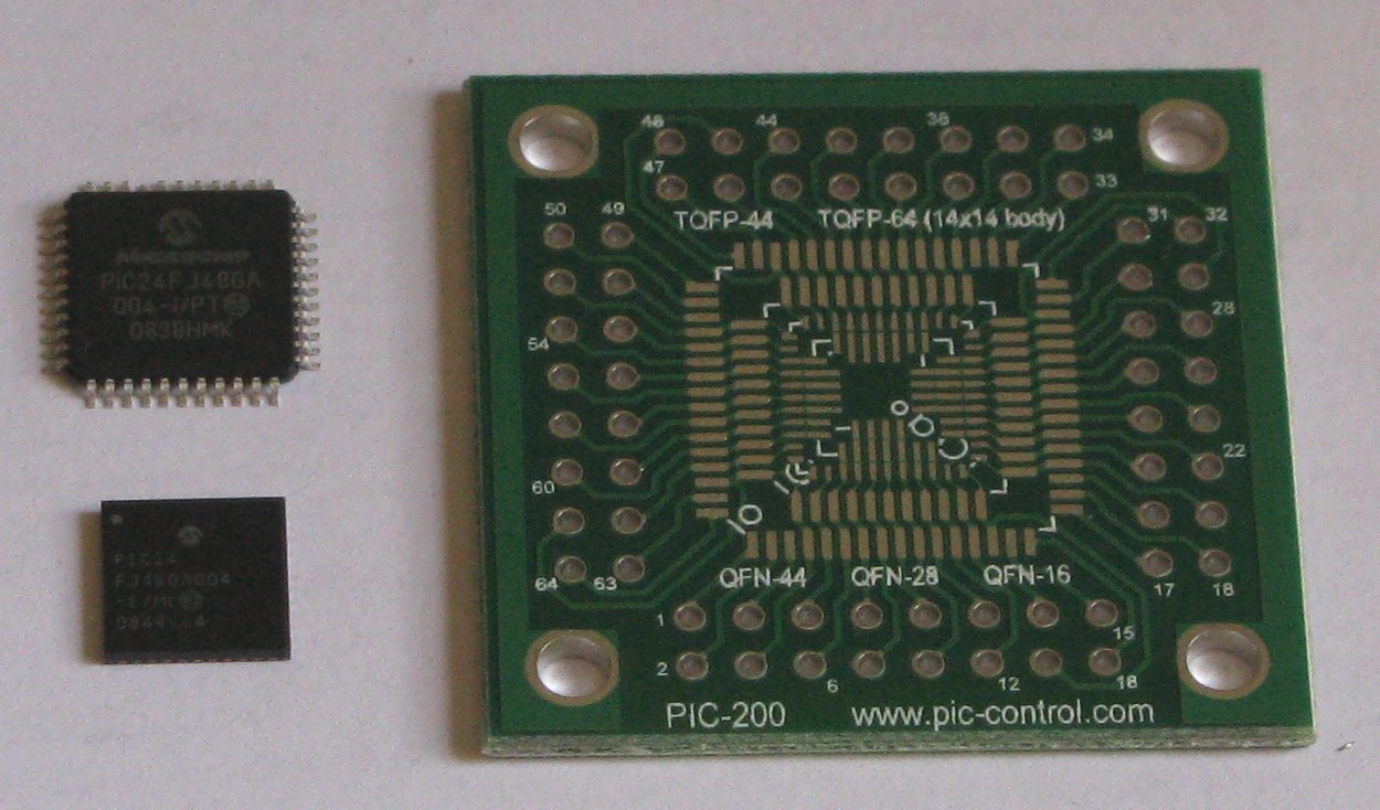
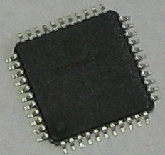
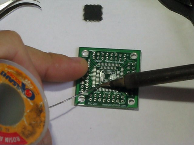
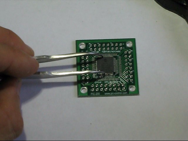
INTRODUCTION In this setup, I am going to solder a surface mount microcontroller (TQFP 44 pins) onto a smd adaptor. The adaptor will then be used on the commonly available prototyping board, so that I can try out my new design for circuit control. TQFP, QFN and SOIC are quite some common footprint for prototyping smd microcontroller from 18 to 64pins. This prototyping adaptor pic-200 (on the left) that I have is an ideal adaptor for my microcontroller. Converting the smd device into 2.54mm, I can easily mount the smd unit onto my 2.54mm pitch prototyping board. It is available locally.
The pic-200 smd adaptor originate from PIC-CONTROL and is well documented. Commonly used smd footprint can be found on either the top or bottom side of the pcb adaptor. These are some of the smd packages that can be mounted onto pic-200 adaptor.
With a wide range of smd components that can be mounted, it is easier to stock up this pcb adaptor for future prototyping use. The following article is about getting my smd microcontroller PIC24FJ64G004 soldered onto this board. After which I will be on my way to do prototyping for my new control circuit. This smd adaptor origined from PIC-CONTROL. For other type of adaptors, you can also refer to other manufacturer as mention above.
|
|||||||||||||||
|
<Step 1>
|
Before soldering, ensure that the soldering pad on the PCB is free of oxidation. PCB is usually tinned to protect the copper surface from oxidation. In cases where the surface is oxidized, you can try cleaning the surface with a contact cleaner. Apply the solution with tissue paper or toothbrush to clean up the contact. This solution make the PCB board rather oily, which I don’t quite appreciate. Contact cleaner.
Let us start our smd soldering here. Soldering surface mount component. The first important thing to introduce would be the solder. There are many type of solder. Choosing the correct solder takes a bit of some knowledge too. Leaded or lead free solder? The industries is moving towards Pb free components & PCB, calling for unleaded product. Lead is toxin and not environmental friendly. I would advise ou to wash your hand after soldering or handling pcb board. A soldering fume extractor to vacuum the smoky fume would be quite comfortable for your soldering. The smoke is quite choking and a health hazard if you breath that in.
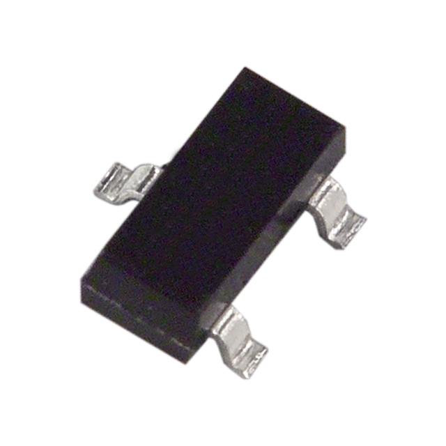
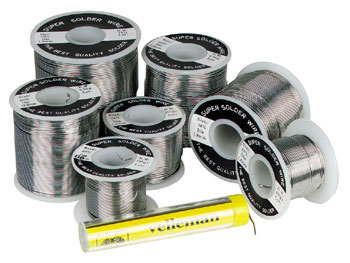
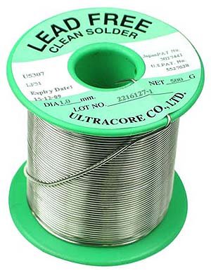
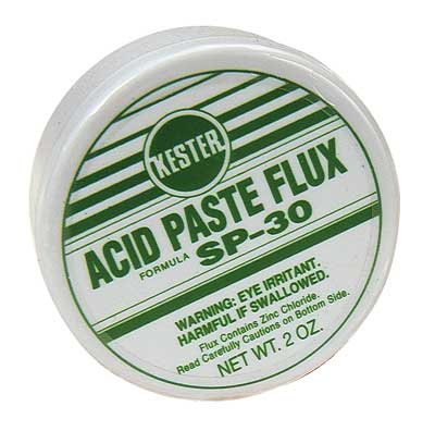
Solder also comes with a variety of metal alloy combination. Nowadays it is common in solder core to contain flux. If the solder do not have the flux in the core, the flux have to be manually applied onto the metal surface before the soldering beginning. The flux cleans up the soldering surface, and also make the solder flow rather smooth like liquid. One of the important ingredient to make a good solder joint lays in the soldering flux. Solder wire also comes in a wide range of diameter to choose from. Generally I use 0.8mm soldering wire roll with flux at the core. Smaller diameter solder wire allows you a better control of the amount of solder to apply. For soldering larger pins or connector component thicker diameter wire will be preferred. Wire too thin is rather troublesome, because you need to feed in a longer length of solder in order to solder the large surface/lead. For general purpose PCB board soldering 0.8mm wire fits somewhere in the middle. Not too thick nor too thin. For smd components, diameter smaller than 0.8mm is preferred. Using 0.8mm for smd soldering is not of any issue.
|
|||||||||||||||
|
<Step 2>
One of the pad being tinned.
Align smd IC to the respective pad.
IC being fixed in position
Checking if alignment is correct.
Flooding the pins with the rest of the solder.
Pins flooded with solder |
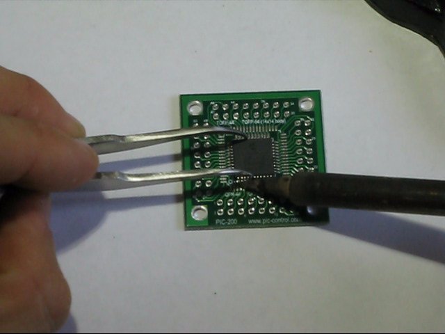
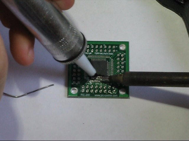
My microcontroller TQFP package has 44pins around the square package. To secure the package to the adaptor, I will need to solder one of the pin to the board first. It is important to solder only one pin. In case of mis-alignment, we can correct it easily. If more pins are soldered, it will be more difficult to correct any alignment. Pin 1 of the adaptor pad is first tinned with a layer of solder. A tweezer is then used to align the IC chip on the pad. The IC is secure to the board with a slight touch from my soldering iron, soldering the IC pin to the pad. The important factor to consider would be the heat generated by the iron. I prefer to use a 60W iron, which still works well in air-con room. A lower wattage or fine tip iron will not heat up that well in colder environment. Goot TQ95 60W
If you prefer a fine tip, perhaps the soldering station will be more suitable. The iron temperature can be adjusted to a higher or precise temperature for the component that you want to solder. Component with thick metal contact like connector, heat sink, for thick cables should be solder with a higher temperature. The iron should be held on longer, in order to have the component fully heated up before any solder is applied.
For soldering the IC pin to the pad, you can start off by heating up the pad. Then while heating up the pad, touch the IC pin and apply the solder wire directly to the pad or IC pin, allowing the solder to flow like liquid. The IC pin is heated last to minimize the chance of over heating the pin. If it doesn’t flow very well, you can manually some flux to the joint. The solder wire should not touch the iron directly, because this will vaporize the flux, and solder flow will be restricted. Heat up the lead and pad longer allows the solder to flow and form a good joint. Not for too long as it can also damaged your IC. You should be able to see the solder flow eventually onto the lead & pad. With a bit of practice, you will see the difference between a quick solder touch and another one with lead & pad heat up a little bit longer. It takes a number of practice to get a good joint with minimum amount of heating time.
The soldering iron that I use has rather thick tip, but that does not matter
when I do soldering for the smd microcontroller. All we do is to flood the
pins with solder. They can be be suck up later. There is a technology known as ultrasonic soldering. The
soldering iron tip has this micro vibration which helps the solder to
flow more easy without much use of flux. It can also solderthose
difficult to solder material. The following is one article that I found
that describe about it. – Soldering the unsolderable.
|
|||||||||||||||
|
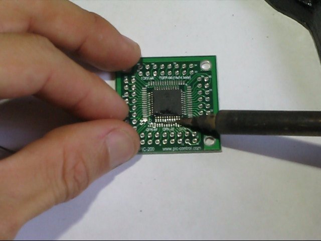
<Step 3>
|
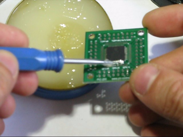
I have applied more flux at this stage. It should have been applied before
flooding the pin, but it doesn’t matter too much. The flux will make the
solder rather liquid so that it is easier to suck up the excess solder.
|
|||||||||||||||
|
<Step 4>
|
The flooded solder is being heated up, and the excess solder are being sucked up. | |||||||||||||||
|
<Step 5>
|
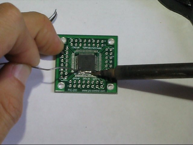
Each pins is being touch up, ensuring that the pin is solder to pad and that
they are not bridged across to the adjacent pins. Now we have got our smd component soldered onto the board. |
|||||||||||||||
|
<Step 6>
|
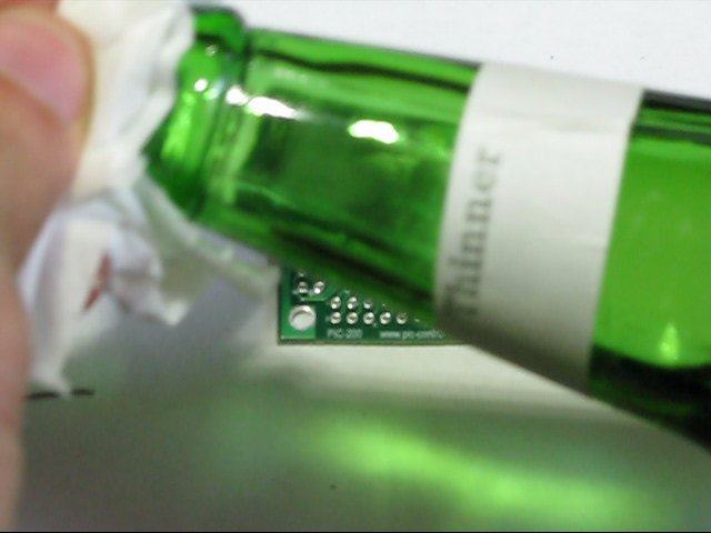
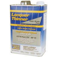
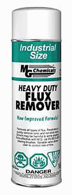
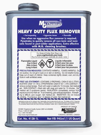
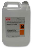
The flux helps a lot in doing a good solder but it often leaves the board with tiny dots of transparent strain, a bit sticky, also known as grease or flux residue. The board looks untidy with these tiny bits of grease. These are the various recommended cleaning solution for pcb. – 50% Alcohol + 50% Water – Thinner – Flux remover – Multicore Prozone MCF800 – Solvent-> Bromopropane; propane, 1-bromo-; propyl bromide (Chemical Formula: C3H7Br)
Besides using chemical, or after using chemical, there may still be some white blur
stain. Those are flux spread dry up on the surface. Using a hot air
blower, or heater on the surface can melt the dry up flux, and recover
the smooth shiny PCB board surface again. Clean away the melt flux
immediate after the heat.
Using alcohol is strongly recommended. Thinner is not suitable for certain plastic/material. Care is required when using thinner for cleaner. Using thinner on the PCB, copper pads and soldering joint isn’t a problem. When use on plastic, you are advise to do a trial to ensure that the material is able to with stand thinner solution. Flux remover is commercially ready mixed solution. From what I learn in the manufacturer website, they are non-flammable chemical solution.
Chemical comes in different level of grade. A slight different in the chemical concentration or purity can results in a large difference in cost. Alcohol can be expensive. For pcb cleaning purpose, request for technical grade alcohol. Higher grade alcohol is typically used for consumption or lab experiment purpose. Since we are using it for cleaning, there is not much advantage in using high quality chemical which is expensive. Dickson chemical is specialized in high graded chemical for laboratory use. They do sell lower cost technical grade alcohol. They are not suitable for consumption but is ok for cleaning application.
You can easily buy thinner from your local hardware. Typically used for cleaning your brushes after all the wall painting works.
These are other recommendation in the web. After researching further, I
would advise not use them. These chemical are of health hazard.
Exposure will have severe adverse health effects. – 50% isopropanol + 50% water – Trichloroethylene – Carbon tetrachloride
Isopropanol (true chemical name) is also known as Isopropyl alcohol or 2-propanol. 2- is refer as Iso. Other chemical may starts with 1- refer as N. These are some jargon used in the chemical industrial. I managed to learn a few of the terms from the vendor. Trichloroethylene (true chemical name) is typically used for degreasing the metal. It is an extraction solvent for oil. Another name for Trichloroethylene is Trielin. Based on some read up, they can cause cancer. http://www.answers.com/topic/trichloroethylene
Carbon tetrachloride can harm our environment, producing CFC which deplete the earth’s ozone layer. http://en.wikipedia.org/wiki/Carbon_tetrachloride
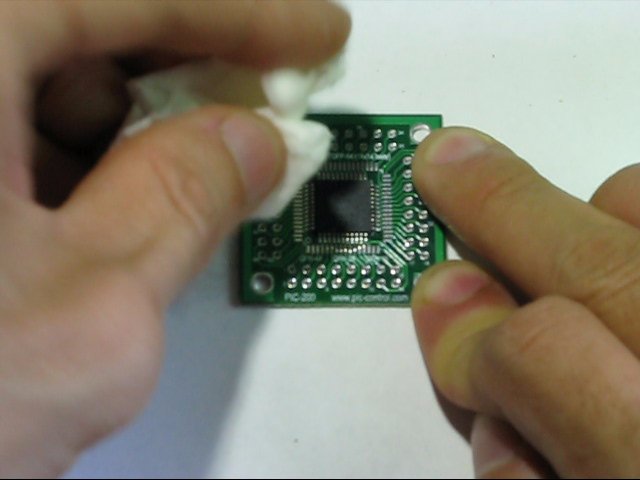
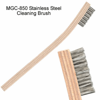
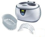
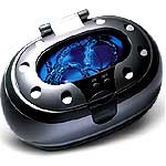
Initially I tried using contact cleaner to clean the stain off. I use cloth or tissue but the fabric is often tear by the component sharp edges. Most corners are not easy to reach. Later on I tried using a toothbrush, the result is better. For mass cleaning job, you can try using the ultrasonic pcb cleaner. It is a deep metal container for the solution, using micro vibration to shake off the dirt. I have never tried on it before, and I believe it is the same machine people used for cleaning their jewelry. Basically, you will need to dip the pcb board into the solution, and the ultrasonic will be activated to do it’s job. The solution used is the same as manual cleaning, requiring 3-5 minutes of cleaning.
Ultrasonic jewelry cleaner
There is also a flux that does not leave residue on the PCB. I found it on the internet, and have not try it before.
Article relating to removing flux residue: – pcb cleaning – Aqueous Cleaning Process.pdf |
|||||||||||||||
|
<Step 7>
|
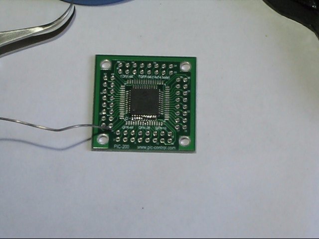
A close up view of the clean and neatly soldered surface mount IC on the prototyping adaptor. Soldering smd components is simple and fast with a bit of practice. Small and easy to clean up. There are too many advantage in working with surface mount, compared to through hole components. This is the end of the short demonstration on smd soldering. I hope these article can provide you some insight and confident to start experimenting circuits using surface mount components.
Video available. Please click here,
|
|||||||||||||||
|
Article on smd soldering. – 2010-07 How to Solder Surface-Mount Devices.pdf
|
||||||||||||||||


 Alcohol
& thinner has a lower flash point, and catch fire easily. You have to be
extremely in handling and storing these flammable chemical. Do not store or
work on the chemical near electrical appliances, hot area or things that can
cause spark. Keep your windows open to allow air to circulate while working
with these chemical. They may cause headache, dizziness and uncomfortable
when inhaled.
Alcohol
& thinner has a lower flash point, and catch fire easily. You have to be
extremely in handling and storing these flammable chemical. Do not store or
work on the chemical near electrical appliances, hot area or things that can
cause spark. Keep your windows open to allow air to circulate while working
with these chemical. They may cause headache, dizziness and uncomfortable
when inhaled.


Singapore Customized, custom made Electronics Circuits & Kits
Various Chemical Reference:
Alcohol 70% + Distill Water 30%
MDX4-4159
7MHFE-71DE
Cyclohexanone
Methylethylketone
ethylacetate,
Silicon Wacker
Wacker M4503, General purpose mould making silicon (Using Two Part Silicon Mold Putty to Make Molds)
http://www.kirkside.com.au/, Mould Material Specialist
Propanol, used to clean PCB. (close to white electric oil)
Acetone, remove away ink printed on PVC stickers
n-Hexane (white electric oil)
smd glue for surface mount component mounting / soldering use
Seal-glo NE series, NE3000S, NE8800T, more Seal-glo
Keyword: surface mount soldering, smd adaptor, smd to 2.54mm convertor