Your reference guide for PCB (trace resistivity, footprint) wire (gaage chart), mil/ inch/mm, hole (drill, tap chart), fastener
Edited by Lim Siong Boon, last dated 02-Oct-09.
Shortcut to your reference guides and charts
- PCB Trace reference
- Wire and Cable gauge
- Advance conductor
- PCB Footprint reference
- Tap drilling guide (mm chart)
- Common Connector Pin Out
- Name of Connectors/Plugs
- Name of Cable/Wire
I always have to refer to these dimension references frequently,
and decide to put them up once and for all on this website.
Hope they are useful to you too.
|
Trace resistance guide based on PCB board 1oz copper at temperature 100˚C. (worst case)
Conversion calculator might not work on some web browser.
Unit conversion table & calculator between inch, mil, mm, oz.
Conversion calculator might not work on some web browser.
also Download the wire gauge calculator from UltraCAD Design, Inc
|
The IC chips, active
and passive components are all connected by traces or wire. The traces
on the PCB are assume to be of short circuit, which is 0Ω. This assumption is reasonable if it
conduct a very small amount of current. When the conductor starts to
carry larger amount of current, the voltage drop across the trace could
be significant, causing intermediate hardware problem.
If you are expecting a large current flowing through the traces, you have to keep in mind to provide a wider trace to increase the conductivity of the cable. Larger trace width means lower resistance. For my PCB route software, the defined trace width for power is 1.27mm and signal is 0.38mm. Sometimes there is a need to route the trace through narrow space. In this situation, I would have to use the recommended trace width for power min, and signal min. Usually I will keep this narrow trace as short as possible to avoid higher resistance. Seldom do I need to worry about traces carrying signal information. I am more worried about the conductor distributing the dc supply to individual circuit zone. Whenever possible, I would provide a wider traces for my 5V and ground supply. When designing the PCB routing for my power supply, I would use the star topologies. This will ensure a evenly spread for the current distribution, hence lowering the burden of individual traces. I have actually experience such technical issue during my final year school project. The noise problem is somehow reduce after the attempt to improve on the trace routing. Another experience involve power up a remote system about 10m away. The distance is quite near and the power cable is rather thick to me. The voltage at the remote end is found to be too low to power the remote system. We have to double the cable conductor in order to resolved the problem. Our equipment conduct high current of about 20A if I remember correctly. The problem might not be obvious because the high current being drawn might happen during certain hard to determine event. For example, when your system trigger the lightings or motor which draws very high current for a short period of time. The voltage drop cause by the sudden high current draw might cause your system to fail. Therefore the design should always cater for the worst case. Always find out the maximum possible current drawn. Over design the system to ensure that the system will not fail in the worst case scenario. Just to make a note, that I have been referring to dc voltage supply. For high voltage AC supply, I guess it is a different way of looking at it. My understanding in high voltage system is quite weak. On the left is the reference table to estimate the resistance of the trace for my PCB routing. I have assume the worst case at temperature 100˚C with the copper layer of 1oz thick. Seldom do you need to refer to this table, unless you have encounter space restriction for your high current carrying traces. It is my usual practise to double the current carrying capacity. 2 times the maximum current I will be expecting. If you have the space, make it wider. |
|||||||||||||||||||||||||||||||||||||||||||||||||
|
Electrical Resistance Equations: Resistance = Resistivity x Length/Area
Question 1: 1oz copper PCB, Trace width 0.25mm, Trace length 0.1m, Operating temperature 25˚C
Solution 1: Copper resistivity at 25˚C is 1.68×10⁻⁸Ω.m Resistance = 1.7×10⁻⁸Ω.m x 0.1m / (1oz x 0.25mm) = 1.7×10⁻⁸Ω.m x 0.1m / (35um x 0.25mm) = 1.7×10⁻⁸Ω.m x 0.1m / (8.75nm2) = 1.7×10⁻⁸Ω.m x 0.0114×10⁹m-1 = 0.19Ω
Question 2: 1oz copper PCB, Trace width 0.25mm, Trace length 0.1m, Operating temperature 100˚C
Solution 2: Copper resistivity at 100˚C is 2.17×10⁻⁸Ω.m, Resistance = 2.2×10⁻⁸Ω.m x 0.1m / (1oz x 0.25mm) = 2.2×10⁻⁸Ω.m x 0.0114×10⁹m-1 = 0.25Ω
|
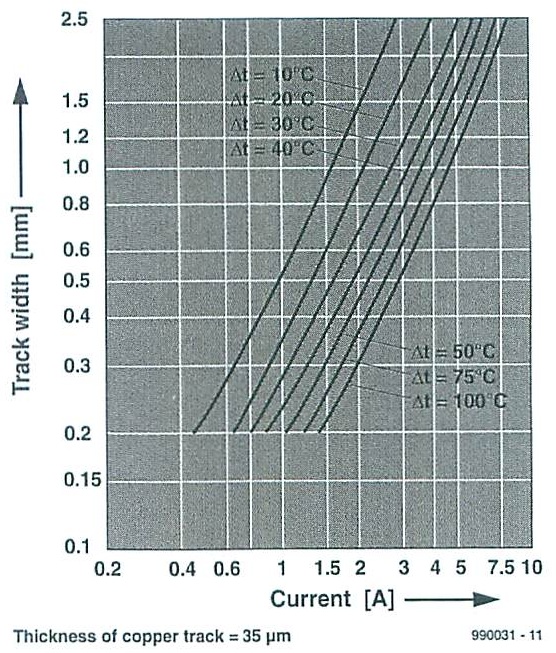
I have also provide the computation for copper resistance for your reference. Taking this opportunity to do further read up in order to explain in a simplified form. Area is the cross sectional area of the conductor. Just like a water pipe, the larger the cross sectional area, the easier the current is able to flow through. Resistivity defines the resistance of the material for a unit of length at a certain temperature. The resistivity for the material copper at 25˚C is found to be 1.7×10⁻⁸Ω.m The resistivity changes with temperature. The resistance will increase as the temperature increase. The term for this changing resistivity with temperature is known as the thermal resistivity of that particular material. The material resistivity would therefore look like a graph curve. They are obtained through test and experiment. For some material, the graph curve could be approximated in the form of equation. This complicated formula describe the resistance behavior of the material under different temperature condition. For copper material, it can be represented from the following equation, Copper resistivity = ρ0(1+α(Temperature-T0)) = 1.7×10⁻⁸Ω.m x (1 + 3.9×10⁻³Ω/˚C x (100˚C-25˚C)) = 2.2×10⁻⁸Ω.m at a temperature of 100˚C <ρ0 is the material resistivity at T0 temperature> As you can see from the calculation on the left, the increase in temperature from 25˚C to 100˚C has increase the 0.1m copper trace by 0.06Ω. This is about 30% increase in the resistance. To keep the topic simple, we will not go into the details of varying temperature. There can be other factor that can affect the resistance of the material. Here is a quick and simple graph showing the change in temperature in relation with the trace width and the current flowing through it. (taken from the magazine elektor 2010-02). The graph assume the pcb copper trace thickness to be 35um (1oz) & that it is place in a open air environment (not enclosed inside a box/casing). For example, given the trace width of 0.6mm, and a 1.5A current flowing through it, we can expect the copper area to rise by another 10°C.
Some article reference: PCB trace – HwB, trace vs current graph.pdf
|
|||||||||||||||||||||||||||||||||||||||||||||||||
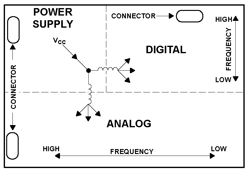
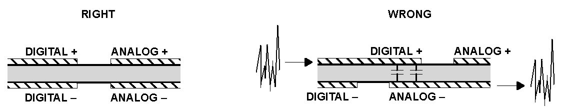
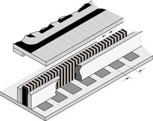
Recommended digital and analog circuit layout on a PCB board.
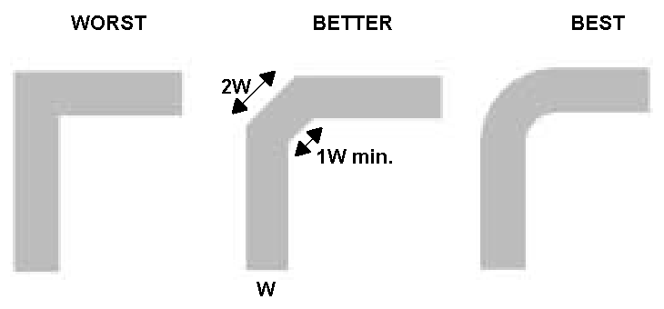
Recommended trace corner layout.
Recommended plane placement.
|
Reference taken from “Op Amps for Everyone“. More PCB layout recommendation can be found in the book “Op Amps for Everyone” from Texas Instruments. |


|
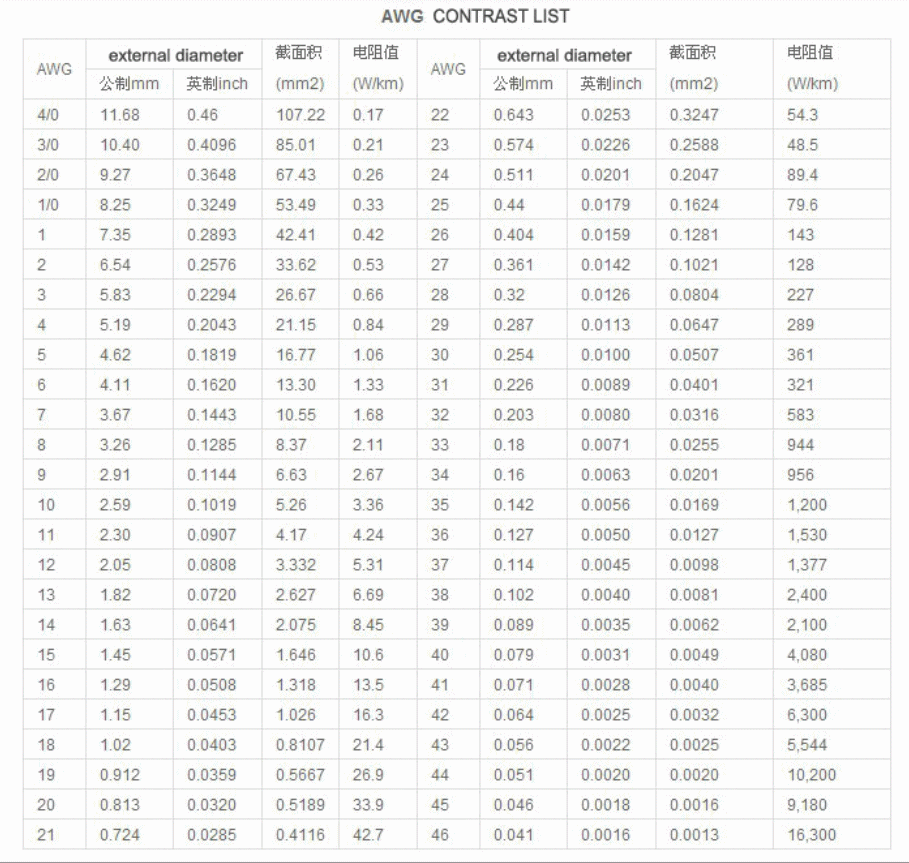
I have put up this wire gauge guide for my own reference. Very often there is a need to return to this reference to choose an appropriate cable for use. I have also written an article some time back. Myth about how the cable relate to their resistance. It is taken out from the main webpage but I have place a link here, for anyone who are interested to understand more. NOTE: The following guideline is a brief guideline for copper ampacity (current rating or current-carrying capacity) of the cable used for power supplying purpose. The ampacity is defined as the maximum current the cable can withstand. Any current higher than that will generate enough heat to burn away the cable. There are many factor affecting the current capacity of the cable, and it should be compensated accordingly. I would advise to select the cable, with at least double the current-carrying capacity for the intended equipment. Never operate near the cable current-capacity limits. You will never know when, the current overruns. Some of the factors that will affect the current-carrying capacity of a cable are: – Conductive wire cross section area. – Wire material. The temperature the material can withstand without melting out. – Temperature. If the wire/insulator jacket can withstand higher temperature, the cable is able to carry more current. – place of installation or the surrounding temperature. – material of insulation jacket/skin/cover. – how much the cable can dissipate heat – Stranded or solid wire type. Stranded wire can carry more current than a solid wire for AC type of signal/power. This is due to a phenomenon known as skin effect.
Reference: – ayenbee AWG Wire Current Rating guide.pdf – Wire Chart for 12Volt 24Volt.pdf – A Guide to Wire and Cable Construction.pdf 230v Cable Size Selector- http://www.electacourse.com/cableselector.html
The factors involve are quite complex. The table is a simplified reference for myself to select the cables. Always allow a larger safety margin of minimum x2 when you chose your cable. Do take careful note of what you deploy.? There are many other factor, eg screw connections, plug contact which will affects the results. If the cable has the slightest warm, it is quite clear that the cable will be hitting it’s limit any time soon.
Cable Guide (typical cable type and name) Click the chart for enlarge view. Chart and images taken from
Other reference, http://www.wiki.diyfaq.org.uk/index.php?title=Cables#Cable_Sizes
|
 230Vac power cable 16mm2 (absolute maximum 69A)
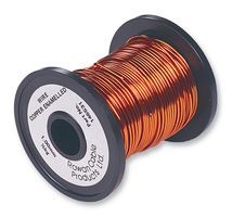
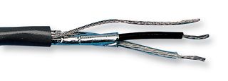 Audio cable (shielded), Belden 8760
 Category 5E network cable, 8060-OZZ7FNL from
Alcatel
Category 5E network cable, 8060-OZZ7FNL from
Alcatel
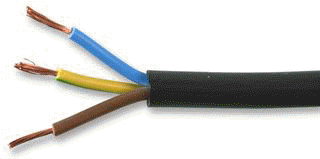
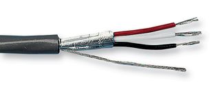 Multipurpose 10core shielded.
(RS232 communication, data signal), Belden 9540, Belden 9536 (6 core),
Belden 9534 (4 core)
Multipurpose 10core shielded.
(RS232 communication, data signal), Belden 9540, Belden 9536 (6 core),
Belden 9534 (4 core) Category 5E network cable
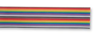 Ribbon cable, 1.27mm
pitch
Ribbon cable, 1.27mm
pitch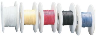 Wire wrapping wire, Ok Industries
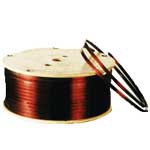 Wire copper enameled
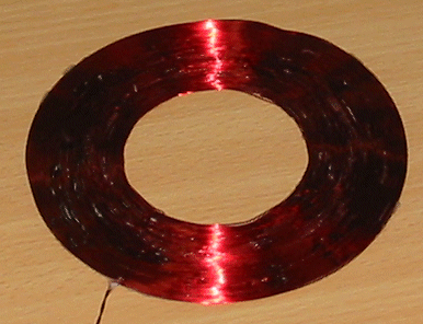
 Wire
copper enameled (very fine)
Wire
copper enameled (very fine)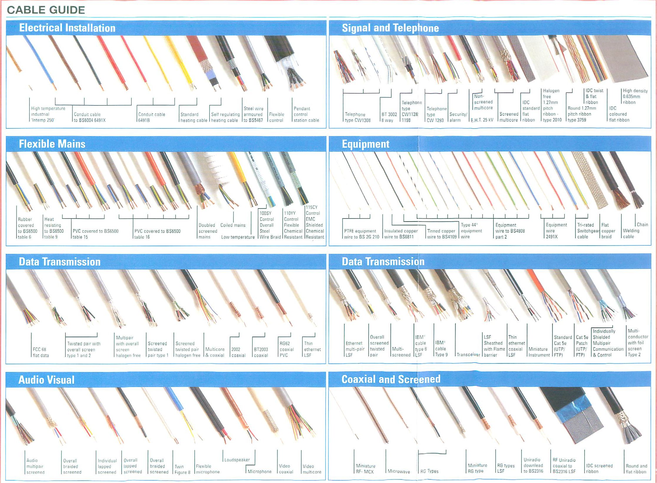
| 3. Advance conductor
Special material for conductivity connection. Some references for non-traditional or advance conductor materials. |
|
|
I happen to see some special wire product that I think I should put them in this website for reference. The follow shows a rubber strip (a black layer sandwich in between the two white layer). It is call the elastomer connector. It is typically used to connect a flat LCD display panel to the pcb board without any soldering. It is quite cool when it was being shown to me for the first time. The LCD and pcb is connected with this elastomer connector sandwich in between. Elastomer connector (soft rubber strip that can conduct like a wire)
|
|
|
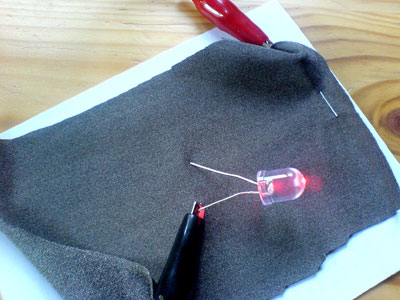
Conductive fabric or cloth The conductive fabric actually can feels like a typical cotton cloth material. Some other feels like a nylon fabric, a bit like plastic. This is great for RF shielding, which we used it to test the performance of RF transmission through various material.
|
|
|
Conductive glass reference: conductive glass
|
|
|
Conductive paint
|
|
|
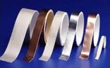
Conductive tapes
|
 this pic is tken from other website


|
|
 Click here to access to footprint
page. Click here to access to footprint
page. |
|
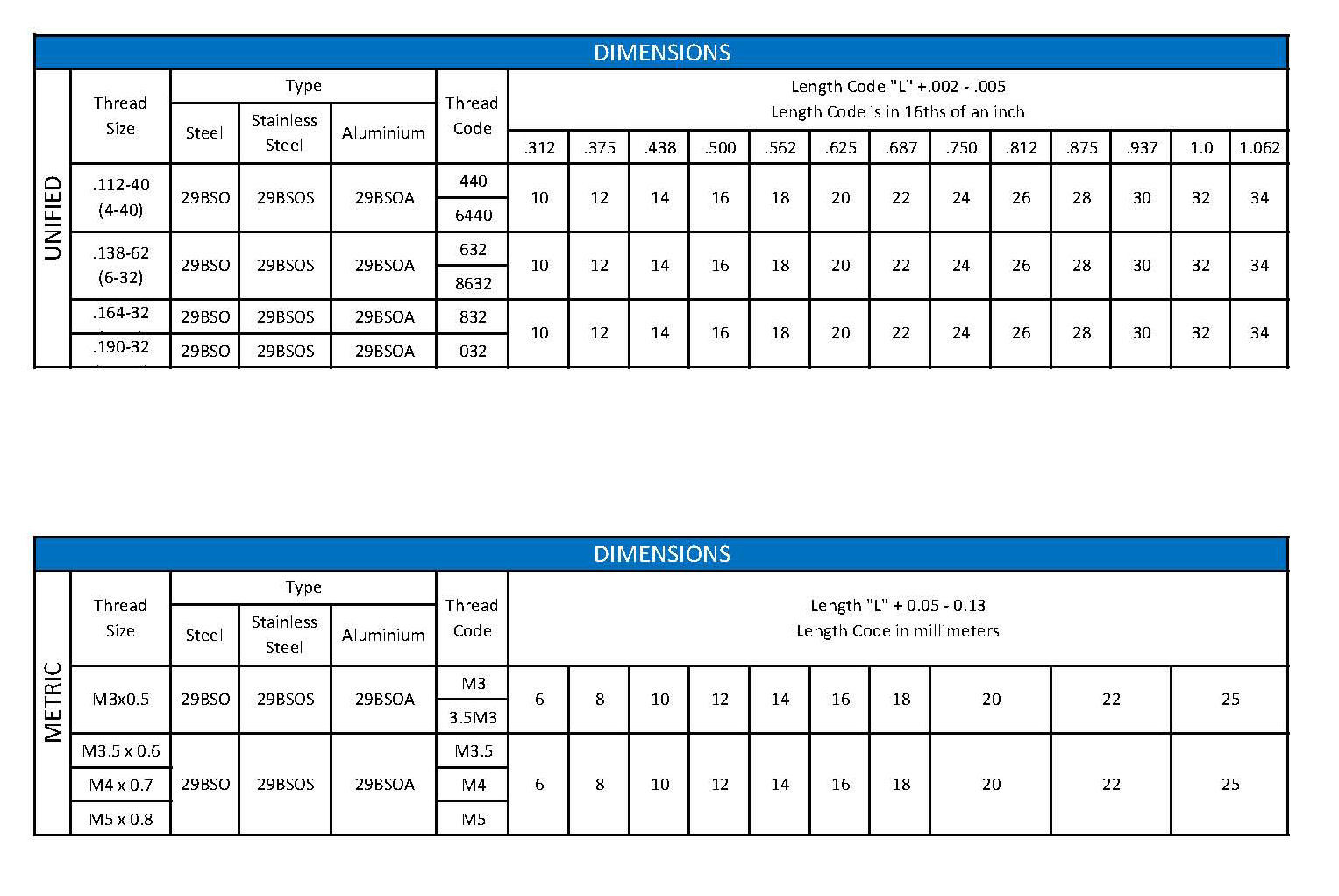
5. Tap drill guide (metric chart) Commonly used screw size in Singapore, Metric (fine pitch)
|
Image of a machine cap screw Enlarge image of the screw thread
->
|
||||||||||||||||||||||||||||||||||||||||||||||||||||||||||||||||||||||||||||||||||||||||||||||||||||||||||||||||||||||||||||||||||||||||||||||||||||||||||||||||||||
| Fastener
Manufacturer:
References: http://www.aboveboardelectronics.com/catalogsmain.htm Fasterner selection guide
Plastic fastener, Cable accessories Enclosure bumper/rubber padding Slide
|
|||||||||||||||||||||||||||||||||||||||||||||||||||||||||||||||||||||||||||||||||||||||||||||||||||||||||||||||||||||||||||||||||||||||||||||||||||||||||||||||||||||
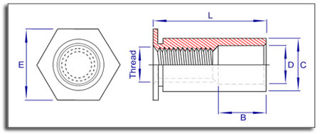
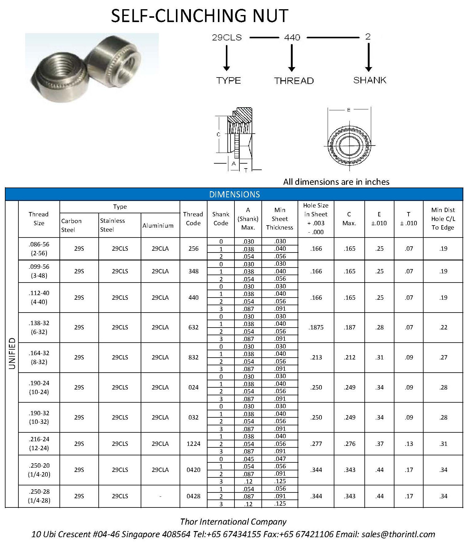
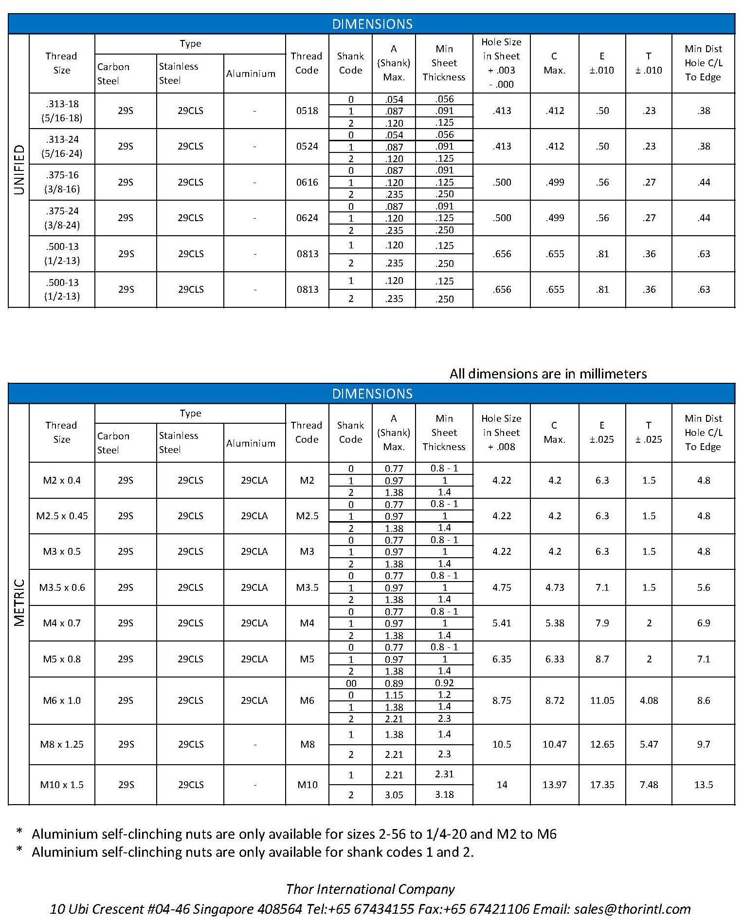
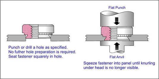
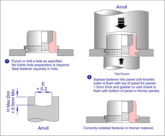
| Self-Clinching Nut, Standoff Guide | |||||||||||||||||||||||||||||||||||||||||||||||||||||||||||||||||||||||||||||||||||||||||||||||||||||||||||||||||||||||||||||||||||||||||||||||||||||||||||||||||||||
Self Clinching Standoff
|
Installation Guide
|
||||||||||||||||||||||||||||||||||||||||||||||||||||||||||||||||||||||||||||||||||||||||||||||||||||||||||||||||||||||||||||||||||||||||||||||||||||||||||||||||||||
Self Clinching Nut
|
Installation Guide
|
||||||||||||||||||||||||||||||||||||||||||||||||||||||||||||||||||||||||||||||||||||||||||||||||||||||||||||||||||||||||||||||||||||||||||||||||||||||||||||||||||||
| Silicone Moldmaking Techniques & Materials | Silicon Moldmaking techniques & material guide.pdf | ||||||||||||||||||||||||||||||||||||||||||||||||||||||||||||||||||||||||||||||||||||||||||||||||||||||||||||||||||||||||||||||||||||||||||||||||||||||||||||||||||||


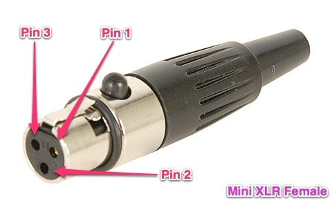
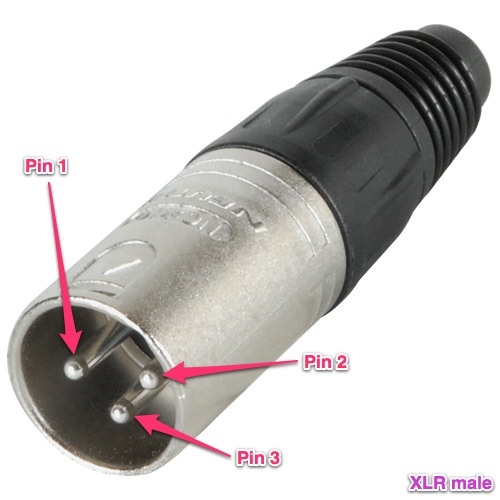
This is a connector pin out reference.
|
|||||||||||||||||||
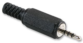
3.5mm 4pins
|
Commonly use for:
Earphone + Microphone: iPhone Mobile Phone Earpiece: Nokia Mobile Phone Earpiece: |
||||||||||||||||||
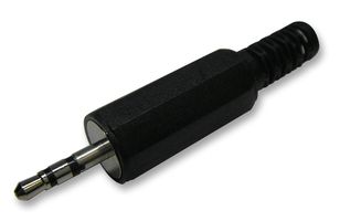
3.5mm 3pins
|
Commonly use for:
Earphone/Speaker pin out: Notes: Speaker’s load is inductive. Measuring the resistivity from the pins will usually yield very low resistance (near to short circuit). Measurement by probing the pin in reverse will yield the same result. Microphone pin out: Earphone/Microphone pin out: |
||||||||||||||||||
3.5mm 2pins
|
Commonly use for:
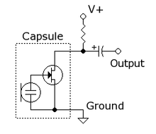
Microphone pin out: Notes: Commonly available electret microphone contains active components. The positive terminal of a microphone can be detected using a ohm meter. Measure Mic+ (+ve Probe), Mic- (-ve Probe) will yield a higher resistivity than probing the reverse way Mic- (+ve Probe), Mic+ (-ve Probe). Electret microphone equivalent circuit
Other type of microphone: reference:
|
||||||||||||||||||
3.5mm 3pins, 2.5mm 3pins
|
Known to be use for: |
||||||||||||||||||
3.5mm 3pins, 2.5mm 2pins
|
Known to be use for: |
||||||||||||||||||
3.5mm 2pins, 2.5mm 3pins
|
Known to be use for: |
||||||||||||||||||
3.5mm 2pins, 2.5mm 2pins
|
Known to be use for: |
||||||||||||||||||
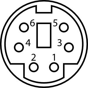
Mini DIN socket 6 pins (female receptacle)
|
Known to be use for:
Walkie Talkie pin out: |
||||||||||||||||||
Mini DIN plug 6 pins (male pins)
|
Known to be use for:
Walkie Talkie pin out: Pin 1- Mic- / PTT Switch common
|
||||||||||||||||||
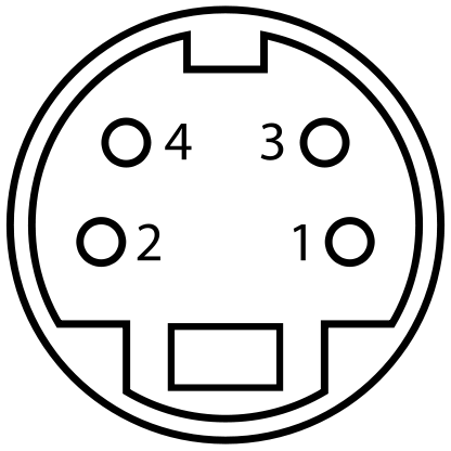
Mini DIN plug 4 pins (male pins)
|
Commonly use for:
Walkie Talkie pin out: |
||||||||||||||||||
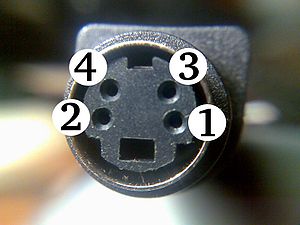
Mini DIN plug 4 pins (female pins)
|
|
||||||||||||||||||
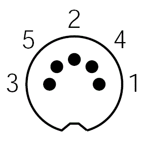
DIN 5 pins
|
Known to be use for:
Bike Audio pin out: |
||||||||||||||||||
|
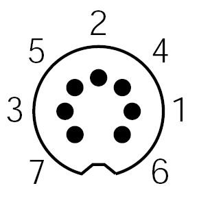
DIN 7 pins
|
Known to be use for:
Bike Audio pin out: |
||||||||||||||||||
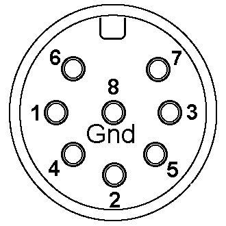
DIN 8 pins
|
|||||||||||||||||||
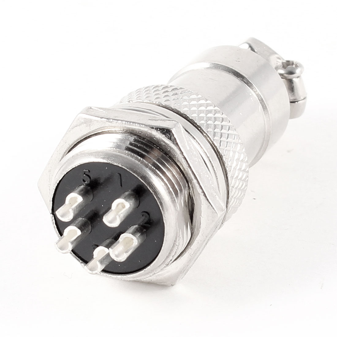
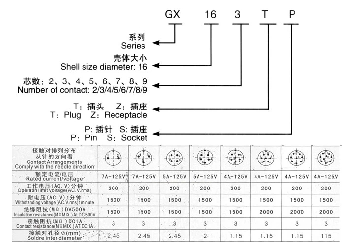
| GX16 Aviation plug and socket connectors (16mm) |
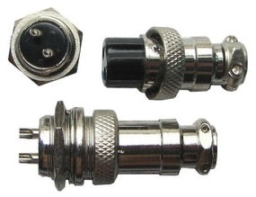 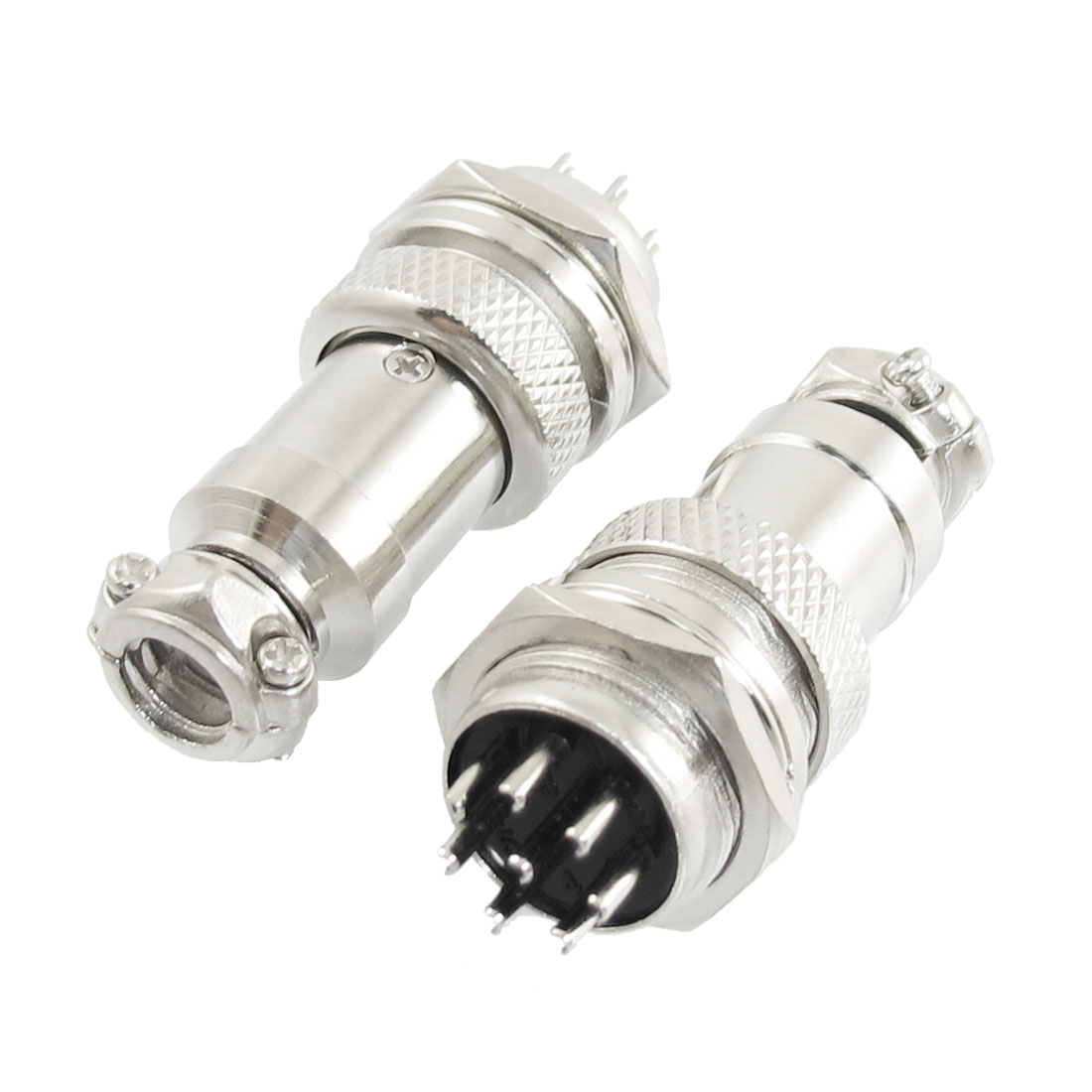 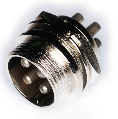       |
||||||||||||||||||
| FD-M16 16mm Connectors |  |
||||||||||||||||||
| Nanaboshi Connectors (panel mount) NJC series (general metallic connectors/socket) NR series (twist lock connector, one-touch lock mechanism) NJW series (waterproof panel mount connectors/socket) |
connector/Nanaboshi%20Connectors%20NJC%20NR%20Series.pdf connector/nanaboshi%20njc%20panel%20mount%20connector.pdf connector/nanaboshi%20connectors.pdf |
||||||||||||||||||
| Amphenol Connectors (panel mount) |
connector/amphenol%20connectors.pdf |
||||||||||||||||||
|
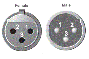
XLR Plug 3 pins
|
Commonly use for:
Studio Microphone pin out: |
||||||||||||||||||
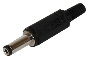
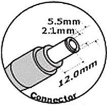
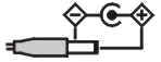
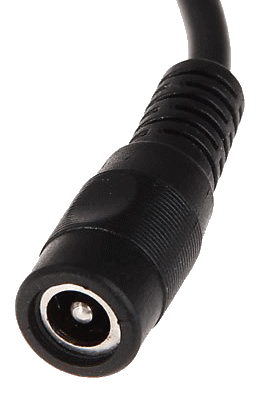
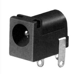
DC barrel jack/socket DC barrel jack (OD=5.5mm, ID=2.1mm, length=11 to 12mm)
DC barrel socket
|
|||||||||||||||||||
|
SMA RF connector (socket for WiFi Antenna)  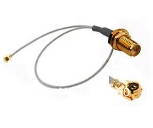 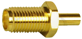 |
Toggle switch dimension, drill hole dimension and thread size 1/4-40 UNS-2A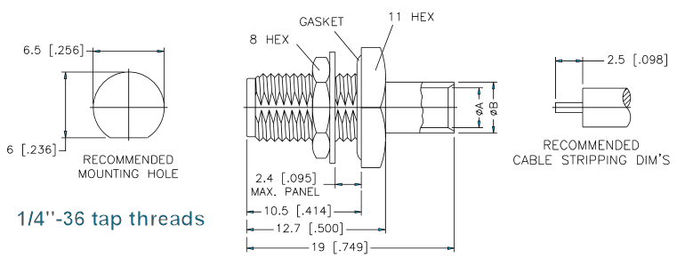 |


|
|
|||||||||||||||||||||||||||||||||||||||||||||||||||||||
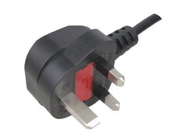
UK 3 pins Plug
|
 |
||||||||||||||||||||||||||||||||||||||||||||||||||||||
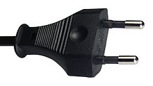
EU 2 pins Plug
|
 |
||||||||||||||||||||||||||||||||||||||||||||||||||||||
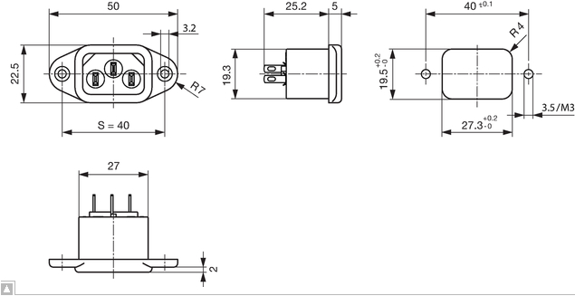
IEC 3 pins Socket
Male Plug -> IEC C14 (picture shown above) Female socket -> IEC C13 Male Plug (with groove) -> IEC C16 Female socket (with groove) -> IEC C15 Check out here for more, |
 |
||||||||||||||||||||||||||||||||||||||||||||||||||||||
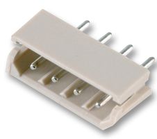
2.54mm pitch |
|
||||||||||||||||||||||||||||||||||||||||||||||||||||||
2.54mm pitch |
|
||||||||||||||||||||||||||||||||||||||||||||||||||||||
TJC8 connector (header and housing/receptacle pins) Another name for housing is receptacle.
|
Pin Header PCB Crimp Style Cable Connector TJC8 series(2.54mm pitch)Wire to Board Crimp style cable P.C.B connector housing terminal pin header 1. Pole: 1-40 Crimping tool, die sets size = ??? |
||||||||||||||||||||||||||||||||||||||||||||||||||||||
JST ZH connectors
SZH-002T-P0.5 (0.08-0.13mm2, AWG28# – 26#, OD 0.8-1.1mm) |
|||||||||||||||||||||||||||||||||||||||||||||||||||||||
JST EL-2P (2 Way) Multipole Connectors With Wire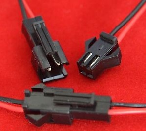 |
|||||||||||||||||||||||||||||||||||||||||||||||||||||||
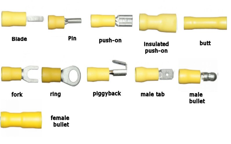   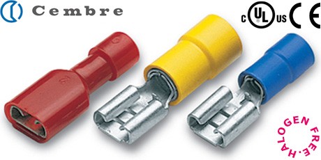 |
Connectors > Crimp Terminals / Solder Terminals & Splices > Quick Disconnect Crimp Terminals Crimp terminal, Blade, Pin, Push-on Insulated push-on, Butt, Fork, Ring, Piggyback, Male tab (6.35mm or 1/4 inch tab connector), Male bullet, Female bullet Red Insulation 0.5-1.5mm2 / 22-16 AWG Blue Insulation 1.5-2.5mm2 / 16-14 AWG Yellow Insulation 4.0-6.0mm2 / 12-10 AWG Good terminal is made of copper (tinned), not aluminium. |
||||||||||||||||||||||||||||||||||||||||||||||||||||||
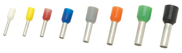 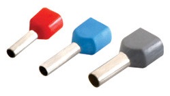  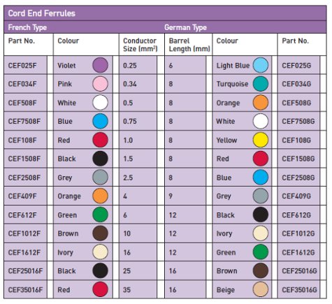 Wire size for various ferrule size (color determine the size) |
Ferrule |

 Molex SPOX 5267 series connector header THT 2.5mm 4 way
 Molex 5263 housing crimp receptacle 2.5mm 4 way
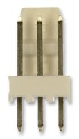 molex KK 6410 series
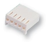 molex KK 6471 crimp receptacle
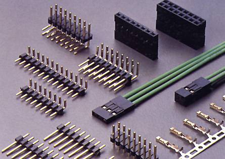

 B3B-ZR(LF)(SN)
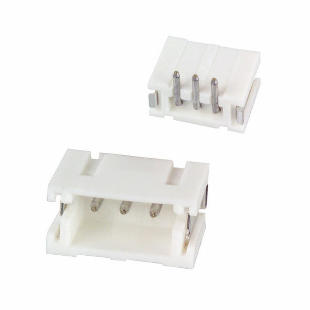 S3B-ZR(LF)(SN)
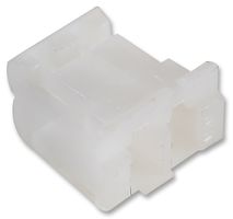
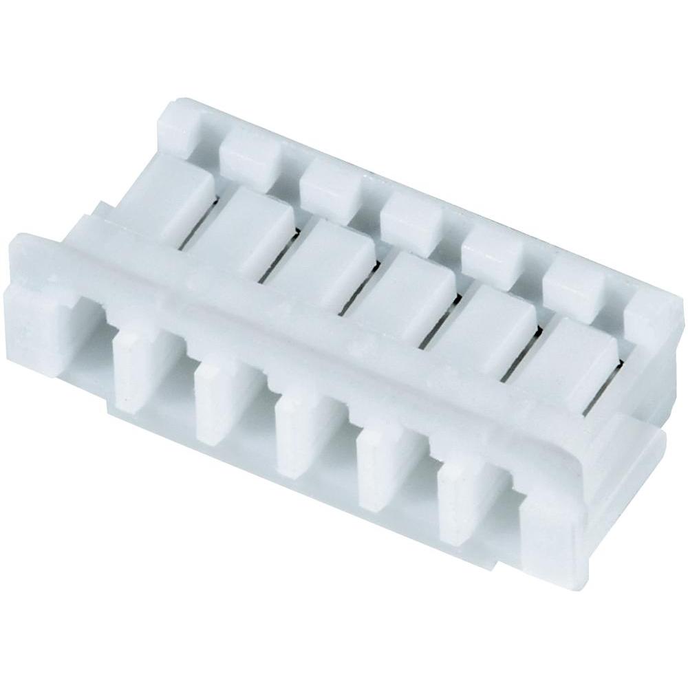 ZHR-3
ZHR-3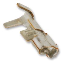 SZH-002T-P0.5
|
|
|
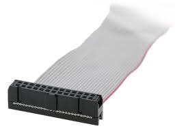
Ribbon Cable & IDE connectors
|
IDC connector pin rating is 1A. |
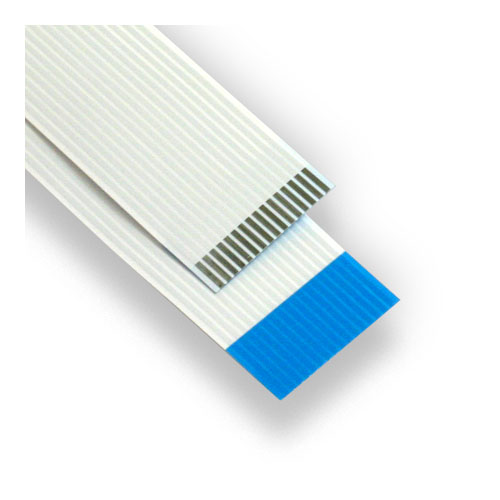
Flat Flexible Cable (FFC)
|
|
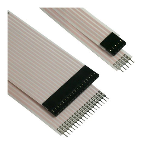
Flex Jumper
|
|
9. Others
|
|
RJ45 (Panel Mount), Ethernet network socket, 8P8C plug to socket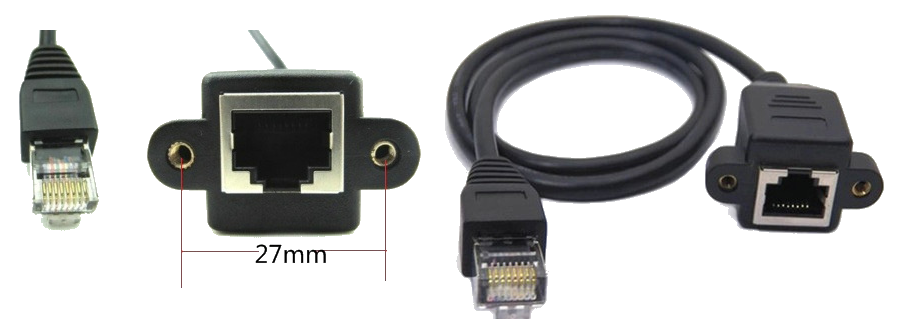 |
|
USB Socket (Panel Mount)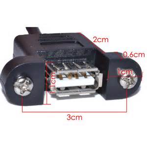 |
|
Keyword: mm inch mil thou, tap drill size, reference guide, PCB trace resistivity computation calculator, Foot print reference, Cable wire gauge resistance, cable wire selection, fastener