|
Reverse engineering circuit
board is definitely not a simply one day training lesson. It is not as
simple as knowing it all simply from a search engine on the internet.
It is a process which harness the years of experience accumulated in
electronic design and studying of how other engineers design their
circuits. While as tough as I may have describe, it does not means that
there is no way to learn this skill.
There are many reason why we need to reverse engineer a circuit board.
One reason that I enjoy doing, is to learn something from the board. In
the early days of my engineering career, as a fresh graduate who have
background about electronics but practically don’t even dare to design
a circuit for commercial use. There was just not enough confident in
myself to design something for the industries to use. It was also a
time when I started to become curious of how a circuit works. As a
fresh new hardware engineer in a R&D department, basically I start
create circuit solution by copying. Copying design that I find from
books, from electronic kits purchase from stores, from internet where
many people uploaded for their projects. I was also fortunate to have a
colleague who had had retired and was working for this small company
that I was working in, who makes me felt like he is nagging, trying his very
best to share his knowledge about electronics with me. Standing there
listening to him teaching from the very basic, starting from the
name of a component. Topic like, how to classify the type of switch
SPST DPST DPDT,can seems boring. It can be quite an annoying thing,
when he speaks about simple things (which I thought they were). The
truth is those simple thing that I thought they were, are actually
fundamentally important, I had realized. Over time I started to earn
some insight which I didn’t really catch then during my polytechnic and
university school days. The topic “Switch”
that I wrote in another webpage is one of the simplest and most
important topic that I think all electronic hardware engineer needs to
know by hard.
Reverse engineering can be like looking at a piece of blank at first.
The more newbie you are, the more you do not know where to start
understanding the circuit. In this section, I will briefly go through
the process of how a circuit board can be reverse engineered in a sequential process.
Circuits can looks like an art where almost every circuit seems so
different. The truth is that many circuits are very similar in nature.
There is a pattern that you can find in every circuit. Recognizing
these pattern is important. The more pattern you know, the faster you
are about to decode the circuit. Electronic is physics and physic is
the same across the world we are now living in. People use the same
knowledge, copy the same knowledge, ends up with circuits that are
quite standardize across the design that we can find. First important
concept that we can start with, is to know that there is a standard
circuits in many of the design. Just like a rubber stamp, people tends
not to reinvent the wheel. We design a circuit that works, and keep on
using that same circuit pattern. Whenever we trace out the component
connection, we will try to match these patterns that we are able to
recognizing. As you might have realized by now, the prerequisite to
master the skill of reverse engineering, is the skill of designing
electronic circuits. Like wise the opposite is also true. Both reverse
engineering and circuit design are skills that need to progress hand in
hand.
Why Reverse Engineering?
– to learn how things work.
– to do something new or unique.
– test hardware’s specification, security and weaknesses.
– better control of the system.
– identify design failure, weak components due to current, voltage or heat.
– identify how product can be improved.
Method of hacking and doing reverse engineering
– information gathering
– trace hardware components and connection
– firmware reverse engineering
– external interface analysis
– silicon die analysis (reverse engineering at microscopic level)
– communication monitoring, protocol decoding, Serial, USB, Ethernet,
I2C, SPI, CAN using oscilloscope, logic analyzer, sniffers, software
tools, etc.
reference:
https://media.blackhat.com/bh-dc-11/Grand/BlackHat_DC_2011_Grand-Workshop.pdf
or BlackHat_DC_2011_Grand-Workshop.pdf
Removing Epoxy Encapsulation.
– hot air soften epoxy
– Chemical, MG Chemicals’ 8310 Conformal Coating Stripper (www.mgchemicals.com)
|
2. Recognizing Components
Recognizing all the components on the circuit board.
|
The most basic thing you need to recognize is the electronic components that
you see on the circuit board. As a new engineer, you may find yourself
floated with odd components that you have not seen before. Many newbie
may recognize those component symbol that we read from the schematic,
but may not be able to recognize them in the actual physical form in a
real physical circuit.
The
resistor component alone can comes with many sizes, shapes, and
color. It is important to recognize them, and understand their
differences in characteristic. In school, we usually take resistor as
only a ohm value, and don’t bother about the precision of the
resistor, tolerance, and even wattage is often ignored. In a
practical circuit design, there are reason why some resistor are bigger
or why some are more precision. First thing first, ensure you can
recognize each and every component on the circuit. Knowing their names
and how they are classified can helps you speed up the time needed to
identify them. It is also a reason why through out my other webpages, I
try to use photo, and put down the possible names that can be use to
identify the components. Identify as much
components as you can. Resistor, Capacitor, Inductor, IC chips, fuse,
diode, transistors, connectors, PCB board, etc…
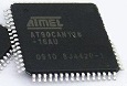
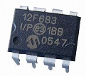
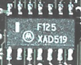
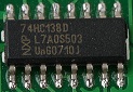
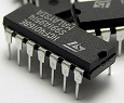
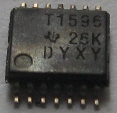
Nowadays, modern circuit board uses more IC chips than passive
components. All IC chip looks the same black encapsulation with various
shape and size. The important thing is to examine the number that is
printed on the chip itself. Without it, you will need more brain power
and experience to decode the board. It is also a main reason why some
manufacturers will find ways to erase the lettering on the IC chips. It
is a means to increase the barrier for reverse engineering, which can
reduce the probability of their circuit design being copied.
With the lettering on the IC chip, you can search for their datasheet
on the internet. If you cannot find them in the search engine, you may
like to try again, leaving out some lettering in the front or back in
order to increase the probability to get a search hit. The latter
section “looking out for the IC chip marking” delicate a section to improve your chance to discover the IC marking and the search for its datasheet.
Most modern circuits are design using surface mount components. They
can be small and traditional color band scheme for a component like
resistor cannot be use. For these SMD resistors, they are number coded.
For bigger SMD resistor, they are number coded,
similar to the color band scheme where the first few digit represent
the actual digit, while the last digit represent the number of zeros.
Smaller SMD resistor which has a smaller printed area print their value
using a standard coded system. This standard coding system is known as EIA marking code.
There is no way to determine the resistor value easily from the code.
Fortunately, we do not have to remember it by hard. With a search
through the internet, we just need to extract its value base on the
code. There is also this free android apps call “ElectroDroid”
which can allow you to key in the EIA code, and return you with the
resistance value. The apps also contains many other features which can
assist you in your reverse engineering process. For more information about resistors and capacitors classification, click on the respective links.
Recognizing the components is only the first step. Identifying
component itself already requires a lot of experience and effort. Even
after nearly two decades of working with electronics, I still do find
components which I find it difficult to identify. Inductor and
transformer is a component which I am still not able to overcome easily.
Newer modern components being used in circuits, often curious me. It is
a never ending learning process.
STEP 1:
Take
a photo of the circuit board (top and bottom), and start to assign a
reference designator (label numbering) for each of the components.
Use OpenOffice Impress to help you do the component part labelling on the photo of the circuit board (PCB).
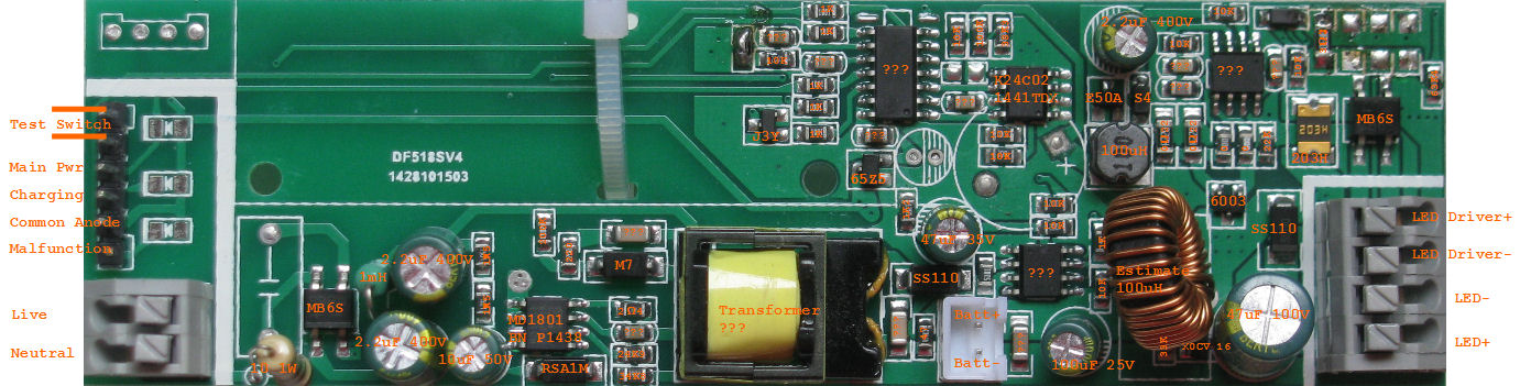
For example, all resistor can have prefix R1, R2, R3, R… R46, capacitors C1, C2, C3, C… C56.
Document these parts on a OpenOffice Calc spread sheet with the following columns,
(S/N or component prefix label, Component type, Package, Marking, Part no., Manufacturers)
Try to fill up the columns with information as much as you can.
You can download a template example here.
– Component reference designator labelling (*.odp)
– BOM list (*.ods)
Check out
STEP 3:
Copy another PCB bottom and extract only the trace or copper area.

Flip the PCB bottom, and size it to be the same size as the top.
The PCB bottom trace adjust the Red & Blue by 50%, so that the trace color can be differentiated from the top pcb trace.
Overlay the PCB top over the PCB bottom. Adjust the transparency of the PCB top to 60%.

This overlay can help you trace the connection without flipping the circuit board physically.
STEP 3:
Build a schematic, laying out the component parts base on those on the BOM list.
STEP 4:
Trace out the connection on the circuit board onto the schematic that you are building.
STEP 5: This
step requires your experience from the circuits that you have seen. It
is sort like a jigsaw puzzle, using your brain pattern recognition
skills, matching component’s connection forming the typical circuits layout that was used.
Arrange the connected components in their typical function configuration layout.
For example the connection may represent a typical
– transistor switch configuration
– input switch and pull-up resistor
– voltage regulator
– amplifier
– output
– etc…
|
3. Mapping out the Traces
Mapping all the traces, the connection on the circuit board.
|
This is the most tedious part of the reverse engineer process. It is to
map out how the components that you have identified earlier are
connected. Component by component, we map out all the connection (known
as traces).
Before starting the tracing process, it is important to recognize the
PCB board type. I classify them as single layer, double layer and
multilayer board.
The simplest board is the single sided PCB where one side of the board
is consist of only the PCB trace routing, while the other side is the
electronic components. Typically consist of mostly through holes
components. Fairly simple to trace out the connection.
The second type is a double layered PCB board where traces can be found
at both side of the board. Most of the time, through hole components
are found on one side of the board while the surface mount component is
found on the other side. Very often, traces are routed below through
hole components and IC chip. This makes it impossible to trace out the
connection using only our vision. Multi-meter’s function “continuity”
is required to aid us to identify a connection (sometimes also known as
the continuity tester). Basically is will buzz when the probes touch
two points which is connected by a trace. You can also use a ohm meter
function which reads a 0ohm when a connection is probed. I prefer the
buzz, because while I focus my attention tracing the circuit, I do not
have to look up in the multimeter screen to check for a connection. The
buzz sound is much more convenient. Although it is a productive feature
to use to trace connection, it is important to note how the
“continuity” feature works. Depending on the multimeter, the buzz is
set to sound at a certain ohm threshold. This means that a 10ohm
resistor between two point, can cause a buzz from the multimeter, which
may mislead you into thinking that the two point is shorted. Do keep
this in mind during the probing process. Using visual and the
continuity features together should help minimize mistake. Components
that you typically need to take note is, sense resistor (usually bigger
in size than the rest of the resistor), inductors, transformer, coil
and any external connection or wiring to the board. Another common
mistake is to probe the circuit without switching off the power supply.
Ensure that all connection to the board are disconnected before tracing
for connection.
The most difficult board to trace will be the multilayer boards.
Typically for a 4 layer boards, most designer likes to allocate the
middle layer for power traces like VCC and GND. It is not a definite,
but just a high possibility base on the experience of looking at other
circuit boards and also some common circuit theory. Doing reverse
engineering requires you to think a lot as if you are the designer
designing the board that you are hacking. For a multilayer board, it
is normally near to impossible to trace the board using visual.
Matching of component pins connection is normally done for the whole of
the circuit board. Matching one pin to the rest of the pin, one at a
time. Sometimes with the understanding of the component, and some
experience as a designer, you might be able to shorten the process.
There will be zones that you will instinctively that there is no need
to try.
Draw out the components position, and how they are connected. Taking a
picture of the circuit helps you to trace easier. Sometimes I will
superimpose the routed trace with the components in order to see the
connection better. Label all the components, and name the trace once
you are able to identify its function.
Power supply traces are the simplest to start with. This is because we
usually knows where the power line is connected to the circuit. From
there we can trace out where the power line goes to. From the power
line, we will be able to trace out the next stage which is typically
the voltage regulators. For a AC power line, usually a rectifier can
be located a before it reaches the voltage regulator. These suggestion
assumes typical design, it will be up to you to recognize it yourself
because there are just too many variation of circuits designed.
Studying the datasheet of the IC chip on board can also help you to
recognize connection. Arrange the component symbol into the standard
stamp circuit configuration that you can recognize. Common standard
circuit like input circuit, pull up, driver circuit using transistor,
relay circuits, voltage regulator, etc… can easily be recognize. Draw
them out in a format that helps you to recognize the circuit module
functionality.
The process is complex, and it is a never ending topics on reverse
engineering. The more you reverse engineer the more you will learn and
improve your techniques, finding new ways to decode and learn how other
circuits are designed.
|