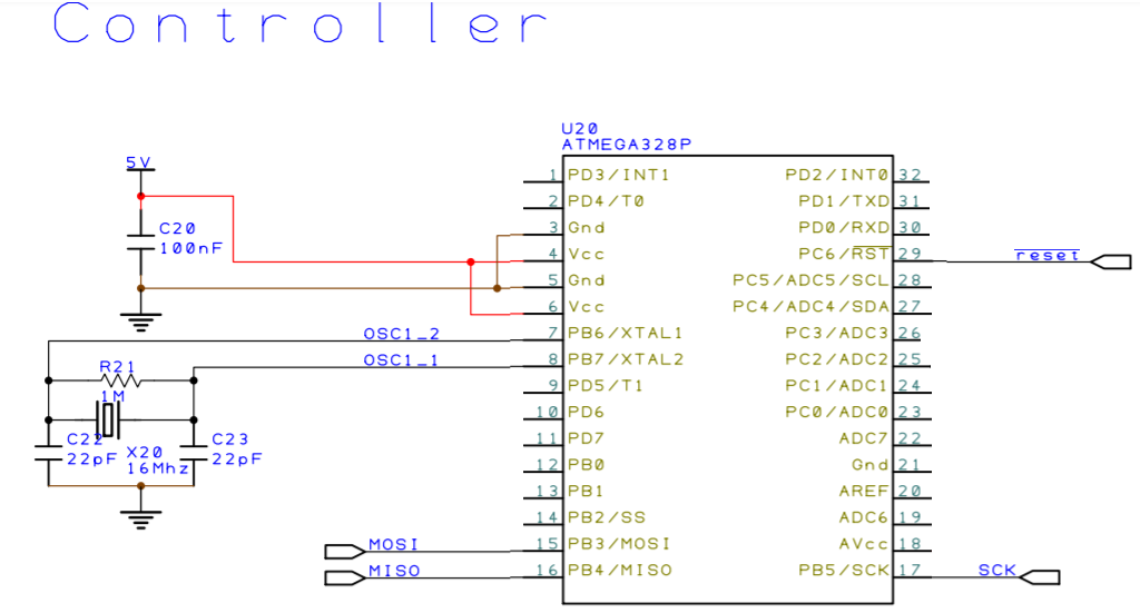
Introduction
This section provides fresh user a step-by-step instruction to upload your updated firmware (a program or machine codes) onto your circuit board using a Microchip microcontroller.

Things That You Need To Prepare
- Your Microchip microcontroller circuit board
- Programmer Tool (PICkit)
- MPLAB X IDE (Integrated Development Environment)
- Firmware (a hex code file *.hex or project files, containing the program of your controller)
Once you are prepared, you can proceed step-by-step to upload your firmware to your microcontroller.
Microchip Circuit Board
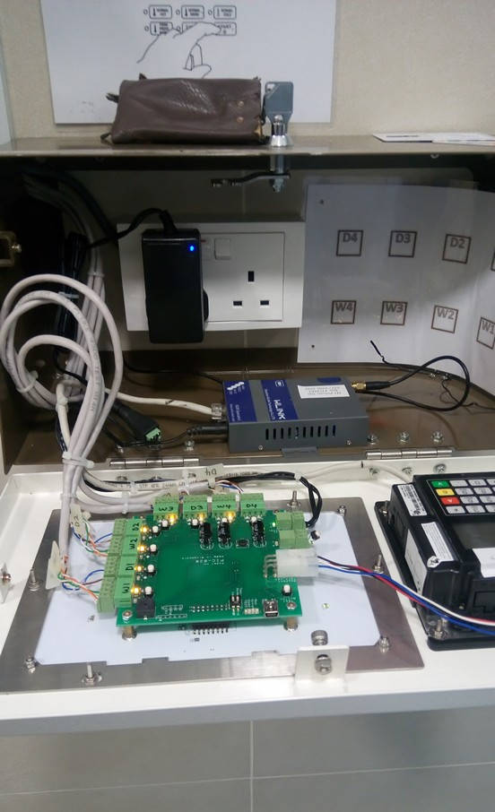
Most microchip circuit board design by PIC-CONTROL comes with a programming port which allows us to upload the program onto the microcontroller chip onboard.
There are standard microchip programming port also known as ICSP, which you can connect to with your programmer tool.
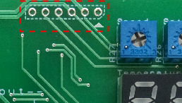
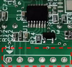
Programming Connector Port on your circuit board product
The programming port is usually located near the edge of your circuit board. It is a row of 6 holes grouped up with a rectangular box (2.54mm pitch header pins).
You must know how to identify the pin no.1 on this port. Pin number 1 of the footprint is indicated by a triangle arrow marking. You can also identify this pin 1 from the bevel corner on the rectangular box.
The following are some photos of how the ICSP programming port looks like on your circuit board.

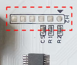 ICSP (a special version without any holes)
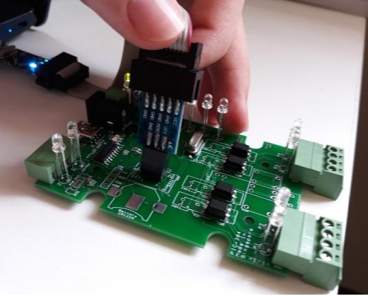
You are suppose to connect the programmer tool to these ICSP port, with alignment to the pin 1.
Details of the procedure will be provided in the later section below.
Programmer Tool
You will need to get yourself a programmer tool. A programmer tools helps you to connect your computer to your microcontroller chip. It is used for uploading of the microcontroller firmware (controller program) onto the microcontroller on your circuit board.
There are a number of programmer tools which allows you to upload your firmware. In this example, we are using the official PICkit 3 or PICkit 4 programming tool from Microchip.
Other commonly known programming tools available are ICD4 (In-Circuit Debugger), ICD3, PM3 and REAL ICE.
Please take note of the pin no.1 on the programmer tool. You must identify this pin and align it to the pin 1 of the ICSP port on your circuit board.
PICkit 3 Programming Tool

PICkit 3
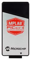
PICkit 4 (new version)
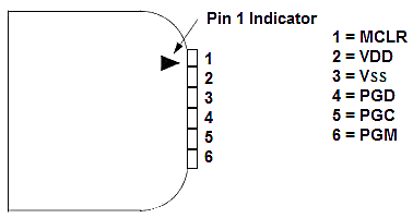
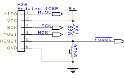
PICkit Programming Tool’s Pin-out
This is the PICkit programmer pin-out. This pin-out is also known as the ICSP programming port.
Please take note that the pin no.1 is identified by the triangular arrow head.
MPLAB X IDE (Integrated Development Environment for Microchip Microcontroller)
The last item that you need is the software which allows you to develop and upload your program to your microcontroller chip.
MPLAB X IDE is a free microchip microcontroller development software. It is a complete platform for your firmware coding development work.
What you should do now is to download the following,
- MPLAB X IDE software (Windows version).
- MPLAB XC Compiler.
Download & Install the MPLAB X IDE Software 
You can click on this shortcut link to download the latest MPLAB X IDE software (Windows version). If this links cannot work, please follow the steps here to download from the Microchip official website.
https://www.microchip.com/mplab/mplab-x-ide
- Click here to go to the Microchip website for MPLAB X IDE software.
- Scroll down to the bottom of the page and look for the “Downloads” tab to click on.
- Go to the respective version (Windows, Linux or Mac) and download the software.
- As of this point in time the software is of version “MPLAB® X IDE v5.05“
Install this software to your computer.
Download & Install the MPLAB X Compiler 
The compiler converts the programming source code into a machine code before you can upload the program into a microcontroller chip. Different microcontroller would requires its respective compiler. It is recommended to install all the compiler as follows.
http://www.microchip.com/mplab/compilers
Install these MPLAB XC8 and MPLAB XC16 compilers to your computer.
Step-by-Step Procedure to Upload Firmware to Microcontroller Chip
Now that you have your
- Circuit Board
- Programmer Tool
- MPLAB X
ready…
We can start to upload your project or *.hex file..
There are two modes of uploading firmware to the microcontroller.
- Method 1: Upload hex.* file (machine code) using MPLAB X IPE software.
- Method 2: Upload project (source code) using MPLAB X IDE software.
Method 1: Firmware upload using IPE Software
This method is usually used for the production. Programmer operators will be provided with a *.hex file for them to upload the firmware to the microcontroller chip.
The advantage of this method is that it is simple, and it do not expose your actual project source code.
Step 1: Launch the program MPLAB X IPE software.
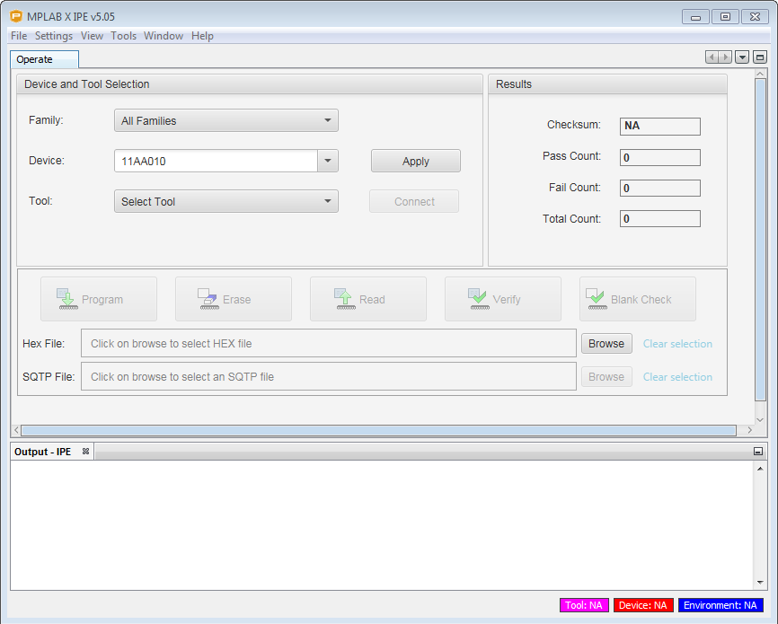
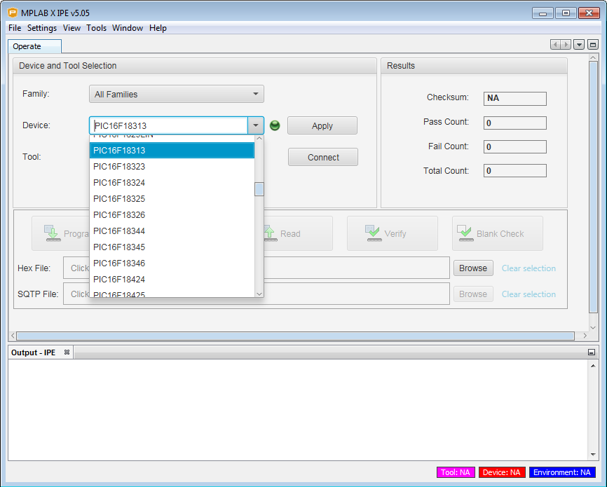
Step 2: Under the section “Device:“, select the microcontroller part number that you want to load your firmware to. Refer to your schematic for the exact microcontroller part number.
Click on the button “Apply“.
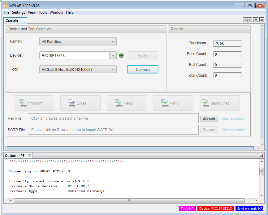
Step 3: Plug in your programmer tool to your computer.
You should notice that the software update the “Tool:” section once your tool is detected.
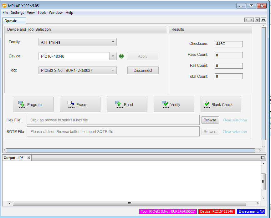
Click on the button “Connect” to start connecting to your programmer.
You should see the following message printed out…
*****************************************************
Connecting to MPLAB PICkit 3…
Currently loaded firmware on PICkit 3
Firmware Suite Version…..01.51.08 *
Firmware type…………..Enhanced Midrange
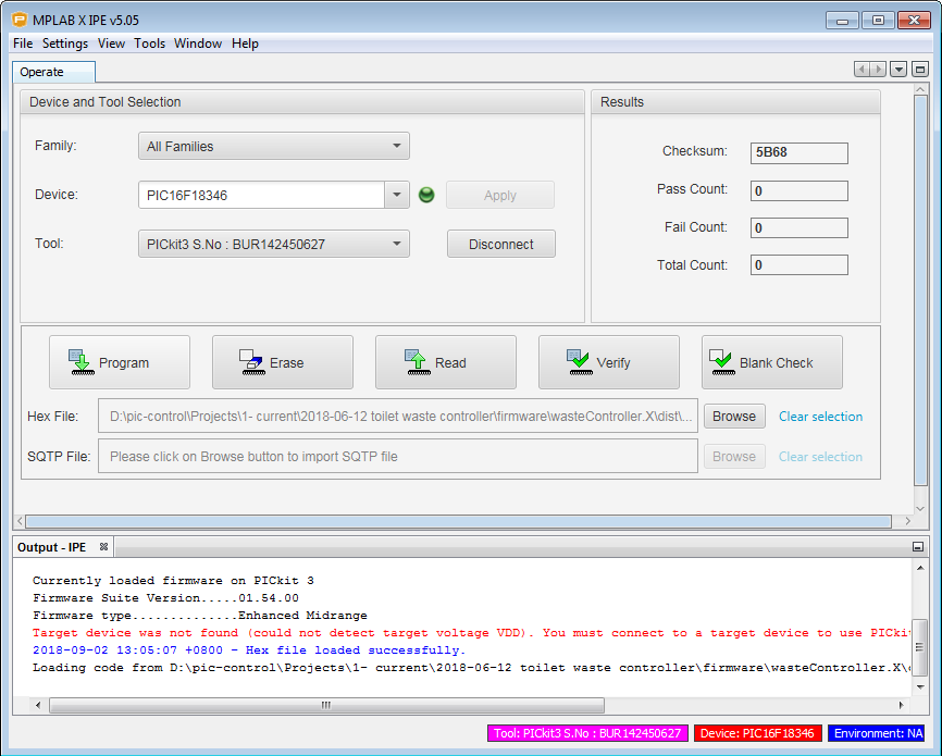
Step 4: Under the section “Hex File:“, load your *.hex file for your production. This is the machine code file for your circuit board. This is the only file required for the production.
For a start, this file is located in your project folder. For example…
Your project directory -> “yourProject.X\dist\default\production\yourProject.X.production.hex“
Step 5: Connect your programmer tool to the ICSP port on your circuit board. Make sure that the pin 1 on your connector is aligned correctly. Then power up your board.
Step 6: Click on the button “Program” to start the uploading of your firmware to the microcontroller chip on your circuit board.
Yes, you are done. Congratulation.
Your board is successfully loaded with the firmware.
Method 2: Project source code upload using IDE Software
This method is usually used during the development. Engineer can edit the source code and upload the firmware changes onto the microcontroller chip directly.
It is recommended to maintain your firmware version while you are doing editing and improvement work. Keeping the original functioning version is a must. You can always fall back on the original copy if you mess up the project source codes.
Step 1: Launch the program MPLAB X IDE software.
Step 2: Open up your project files. Go to File > Open Project…
Select your project files. It is the project folder which ends with *.X. For example “yourProject.X”
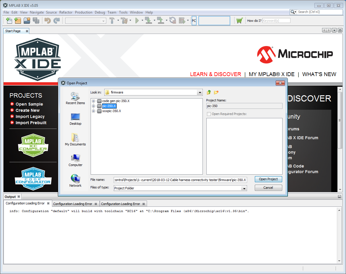
The project will loads up.
Step 3: Plug in your programmer tool to your computer.
Step 4: Connect your programmer tool to the ICSP port on your circuit board.
Make sure that the pin 1 on your connector is aligned correctly. Then power up your board.
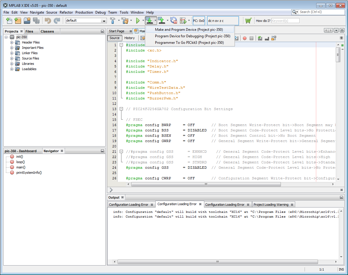
Step 5: Click on the arrow down icon below the menu bar.
Select “Make and Program Device” to start the uploading of your firmware to the microcontroller chip on your circuit board.
Yes, you are done. Congratulation.
Your board is successfully loaded with the firmware.
More…
For further details, you can check up the Microchip official website
or YouTube  for a more detailed instructions.


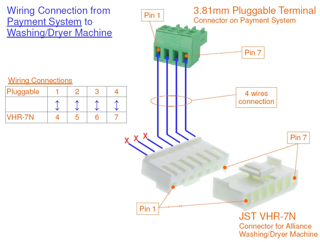


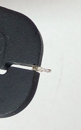
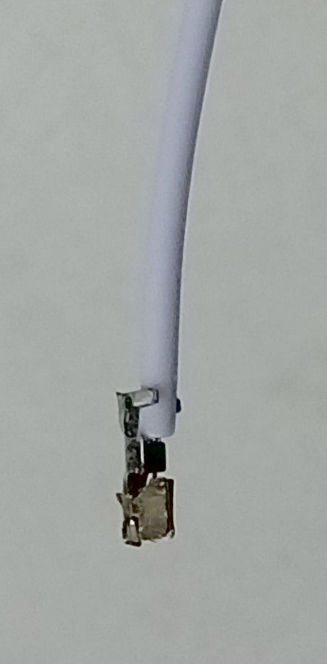
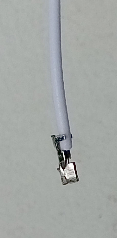
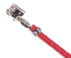
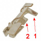 1mm pitch pin for crimping onto wire
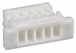 receptacle socket for housing the pins
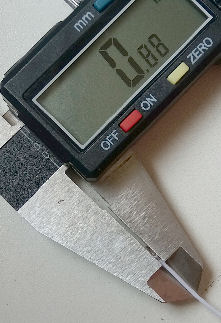
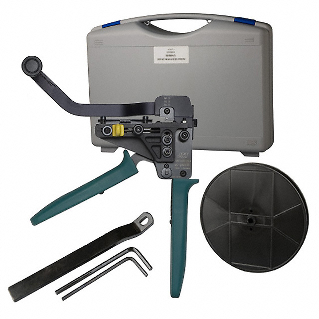 Not only it is small in size, the tool for crimping this 1mm pin is also difficult to find. This tool is rare, hence it is also very expensive. The crimping tool for a